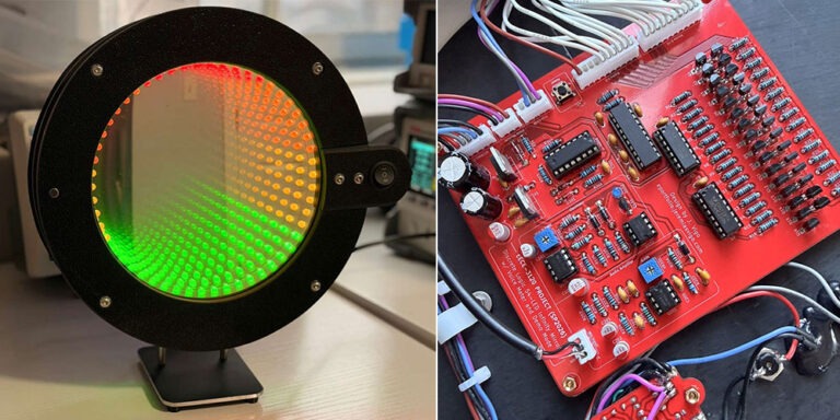
The goal of this project was to design an infinity mirror that converts analog inputs into visual effects using all-hardware, discrete logic design. It uses a low frequency oscillator to produce a predefined waveform used for the “demo mode” display, and a high-sensitivity audio amplifier to convert ambience sounds into a “voice meter” visual effect. The output from both circuits is routed into the input of an ADC0804 analog-to-digital converter (through a mode-switch and a multiplexer), which converts the analog signals to digital outputs used to control the 54 LED display. The main challenge of this design was to intentionally avoid the use of microcontrollers and programable LED strips. Instead, design involved a cascaded, “all-hardware” matrix using only MOSFETs to drive the 54 individual LED display based on each analog input.
System Operation
The overall signal flow is as follows:
- The oscillator generates a very slow analog waveform for demo mode, while the microphone amplifier produces a DC envelope for voice-meter mode.
- The CD4053 multiplexer selects which signal is sent to the ADC input based on the user’s choice.
- The ADC0804 then converts the analog voltage into digital output (8-bits).
- The four MSBs are used by the cascaded 74HC238 decoders to create 16 discrete banks.
- A MOSFET driver matrix expands those banks into a progressive 54-LED radial display.
- An independent PWM circuit controls brightness by modulating the decoder enable line.
The design allowed the project to combine analog conditioning, digital conversion, logic decoding, and power switching into a single hardware system.
Components and Bill of Materials
The project required a mix of analog ICs, logic devices, MOSFETs, passives, connectors, and custom mechanical parts. The main active devices include an LM7805 voltage regulator, ADC0804 converter, two 74HC238 decoders, LM555 timers, LM358 op-amps, and a CD4053B analog multiplexer. The display-driving stage uses sixteen 2N7000 N-channel MOSFETs and fifteen BS250 P-channel MOSFETs, along with an IRF9540N for reverse-polarity protection. Custom mechanical parts include a 3D-printed LED ring, support frames, enclosure panels, and circular plexiglass sheets.
Table 2. BOM List
| Reference | Qty | Value / Type | Description |
|---|---|---|---|
| C1 | 1 | 2200u | Electrolytic Filter Capacitor |
| C1 (PWM) | 1 | 100n | Ceramic Decoupling Capacitor |
| C2 | 1 | 0.1u | Ceramic Bypass Capacitor |
| C2 (PWM) | 1 | 100u | Electrolytic Reservoir Capacitor |
| C3 | 1 | 1000u | Electrolytic Filter Capacitor |
| C3 (PWM) | 1 | 10n | Timing/Control Capacitor |
| C4, C7-C10, C12, C205-C206, C301 | 9 | 0.1u | Ceramic Bypass/Decoupling |
| C4 (PWM) | 1 | 0.1u | Ceramic Timing Capacitor |
| C5, C203-C204 | 3 | 100p | Ceramic Stability Capacitor |
| C6, C11 | 2 | 6.8n | Ceramic Capacitor |
| C13 | 1 | 470u | Electrolytic Filter Capacitor |
| C101 | 1 | 47u | Electrolytic Capacitor |
| C102 | 1 | 100u | Electrolytic Capacitor |
| C201-C202 | 2 | 10u | Electrolytic Capacitor |
| C207 | 1 | 2.2n | Ceramic Capacitor |
| D1 | 1 | 1N4742 | 12V Zener Diode |
| D1, D2 (PWM) | 2 | 1N4148 | Fast Switching Signal Diode |
| D101, D103, D201 | 3 | 1N5817 | Schottky Barrier Rectifier |
| D102 | 1 | LED | Status Indicator |
| D301-D302 | 2 | 1N4148 | Fast Switching Signal Diode |
| R1 (PWM) | 1 | 1k | Fixed Resistor |
| R1-R33, R301-R304 | 37 | 10k | Fixed Pull-up/down Resistor |
| R34 | 1 | 10k | Fixed Resistor |
| R35 | 1 | 1.8k | Fixed Resistor |
| R101 | 1 | 4.7k | Fixed Resistor |
| R102 | 1 | 47k | Fixed Resistor |
| R103 | 1 | 51k | Fixed Resistor |
| R104 | 1 | 75k | Fixed Resistor |
| R105 | 1 | 3.3k | Fixed Resistor |
| R106, R201 | 2 | 2.2k | Fixed Resistor |
| R107 | 1 | 330 | Current Limiting Resistor |
| R202 | 1 | 2M | High Resistance Resistor |
| R203-R204 | 2 | 9.1k | Fixed Resistor |
| R205 | 1 | 150 | Fixed Resistor |
| R206 | 1 | 120 | Fixed Resistor |
| R207 | 1 | 680k | Fixed Resistor |
| VR1 (PWM) | 1 | 10k | Duty Cycle Control Potentiometer |
| VR101 | 1 | 100k | Trimmer Potentiometer |
| VR201 | 1 | 1M | Trimmer Potentiometer |
| Q1-Q16, Q101 | 17 | 2N7000 | N-Channel Signal MOSFET |
| Q17-Q31 | 15 | BS250 | P-Channel Signal MOSFET |
| Q32 | 1 | IRF9540N | P-Channel Power MOSFET |
| U1 | 1 | LM7805 TO220 | +5V Linear Voltage Regulator |
| U1 (PWM) | 1 | LM555xN | Precision Timer (PWM Generator) |
| U2 | 1 | ADC0804LCWM | 8-Bit CMOS A/D Converter |
| U3, U4 | 2 | 74HC238 | 3-to-8 Line Decoder/Demux |
| U101 | 1 | LM555xN | Precision Timer IC |
| U102, U201 | 2 | LM358 | Dual Operational Amplifier |
| U301 | 1 | CD4053B | Analog Multiplexer/Demultiplexer |
| J1 | 1 | DC/SW/LED System Connector | |
| J1 (PWM) | 1 | Connector | 3-Pin Interface Header |
| J2 | 1 | Front SW Connector | |
| J3 | 1 | PWM module | Module Interconnect |
| J4 | 1 | MIC input | Audio Input Jack |
| J5 | 1 | Banks 0-5 | Interface Header |
| J6 | 1 | Banks 6-15 | Interface Header |
| SW1 | 1 | SW Push | Momentary Push Button |
| Front Switch | 1 | DPDT | Toggle Switch 3 Position 3 Pins ON/Off/ON |
| LED ring | 1 | – | 175 mm 3D printed ring |
| Glass Film | 1 | – | Reflective Mirror Glass Film |
| Microphone | 1 | 20-22Khz | Electret Condenser Microphone |
| LED Diode | 53 | 5 mm | |
| Wire | 100 ft | 22AWG | Flexible Wire (LED Array) |
| Rubber feet | 4 | – | 1/2″ Black Round Rubber Feet |
| Brackets | 2 | – | Corner Aluminum Brackets |
| Steel Spacers | 10 | M4 thread | Standoffs and Screws (4 cm long) |
| Main power switch | 1 | SPST | Round Switch SPST 20 mm |
| Power jack | 2 | 5.5×2.1 mm | 2 Pins DC Power Jack Female |
| Plexiglass sheet | 2 | – | 1/8″ Circle 7 Inch Diameter |
| Shielded mic cable | 3 ft | 24AWG | 24AWG Foil Shielded Cable |
Circuit Description
1. Reverse-Polarity Protection and 5 V Regulation
The system begins with a reverse-polarity protection stage followed by a voltage regulator that provides a stable 5 V rail for the rest of the project. The protection stage uses a P-channel MOSFET, a 12 V zener diode for gate protection, a resistor, and filtering capacitors. The LM7805 then regulates the input supply down to 5 V. Large electrolytic capacitors help stabilize the rail, while the smaller bypass capacitors suppress high-frequency noise and help keep the system clean and reliable.
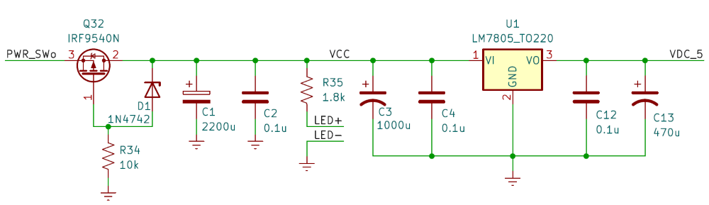
Figure 1. Reverse-polarity protection and LM7805-based 5 V voltage regulation circuit.
2. Low-Frequency Oscillator
Demo mode is driven by an ultra-low-frequency oscillator based on an LM555 timer. The oscillator generates an adjustable sawtooth waveform in the range of about 0.09 Hz to 0.21 Hz. An LM358-based buffer and rectifying stage conditions this signal so the ADC receives a clean 0–5 V envelope. This allows the display to sweep smoothly from the bottom to the top of the mirror.
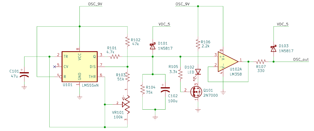
Figure 2. Ultra-low-frequency oscillator and buffer/rectifier stage.
3. Audio Amplifier
In voice-meter mode, an electret microphone captures ambient sound and feeds it into an LM358 amplifier stage. A 1 MΩ potentiometer sets the sensitivity. After amplification, the signal is passed through a rectification and envelope-filtering stage so the output becomes suitable for the ADC input. A clipping diode also limits the voltage to protect the ADC from signals above 5 V.
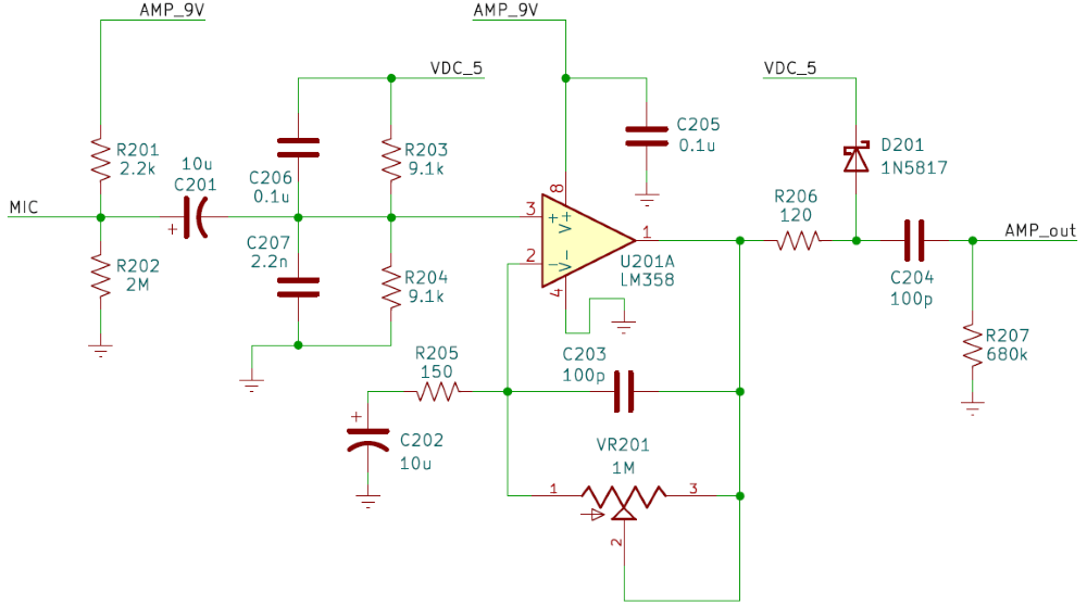
Figure 3. LM358-based microphone audio amplifier with rectification and envelope filtering.
4. Multiplexer Input Selector
A CD4053B analog multiplexer is used to select which conditioned analog signal is sent to the ADC input. In demo mode, the oscillator output is routed to the ADC. In voice mode, the microphone amplifier output is selected instead. In the center OFF position, neither path is actively selected, and the ADC input is pulled low through a resistor so it does not float. This keeps the system stable in every switch position.
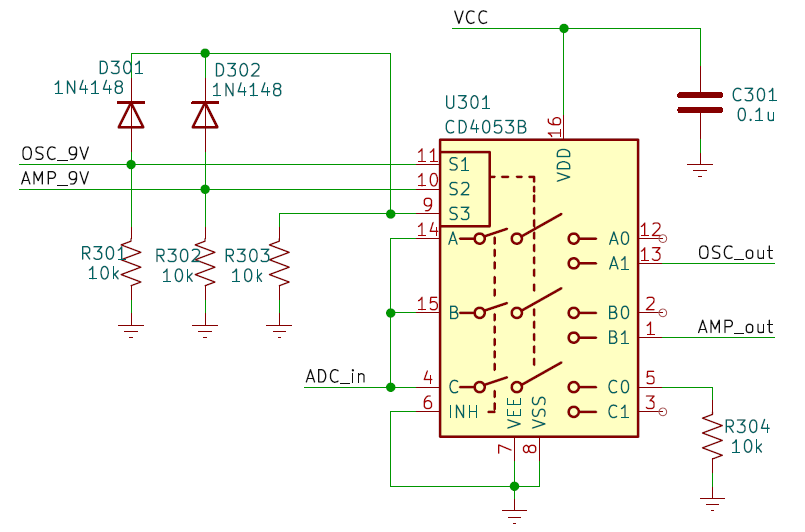
Figure 4. CD4053B multiplexer used to select between oscillator and audio-amplifier inputs.
| Operating Mode | Front Switch Condition | Multiplexer Control Action | Analog Routing | Result on Display |
|---|---|---|---|---|
| Demo Mode | Oscillator ON, amplifier OFF | Oscillator output selected | Oscillator output → ADC input | Automatic sweeping LED pattern |
| Voice Mode | Amplifier ON, oscillator OFF | Amplifier output selected | Amplifier output → ADC input | Sound-responsive meter display |
| Center OFF | Oscillator OFF, amplifier OFF | No signal path selected; ADC input pulled LOW | No signal passed to ADC | Display returns to idle/off state |
5. Logic Architecture and Conversion
The ADC0804 converts the selected analog voltage into 8-bit digital data. For this design, only the four most significant bits are used. These four bits feed two cascaded 74HC238 3-to-8 line decoders, creating 16 display banks. This approach keeps the system simpler while still providing enough resolution for a smooth-looking radial level display.
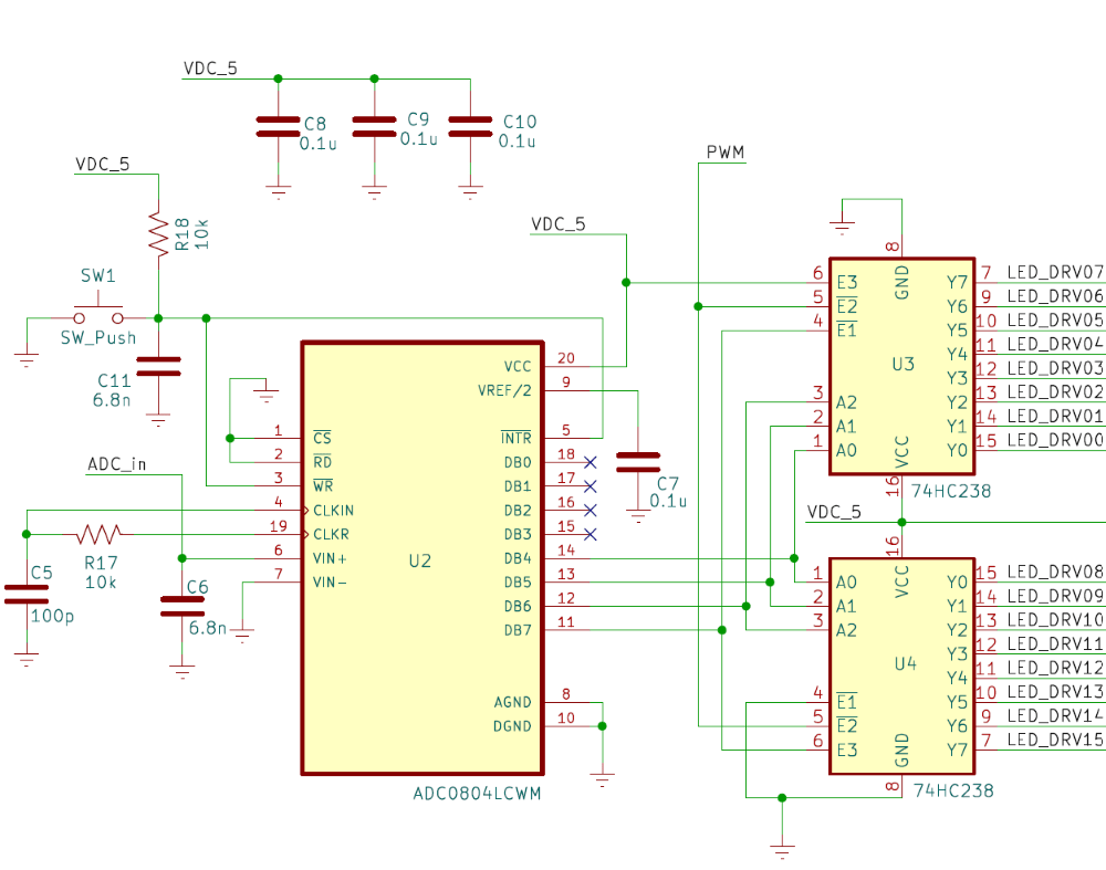
Figure 5. ADC0804 and cascaded 74HC238 decoder architecture.
6. Display Driver Matrix
The 54-LED display is driven by sixteen 2N7000 N-channel MOSFETs, one for each bank. To keep all lower banks on as higher ones activate, fifteen BS250 P-channel MOSFETs are used in a bridge network. This creates the cumulative lighting behavior needed for the mirror to fill up progressively instead of only showing a single active level.
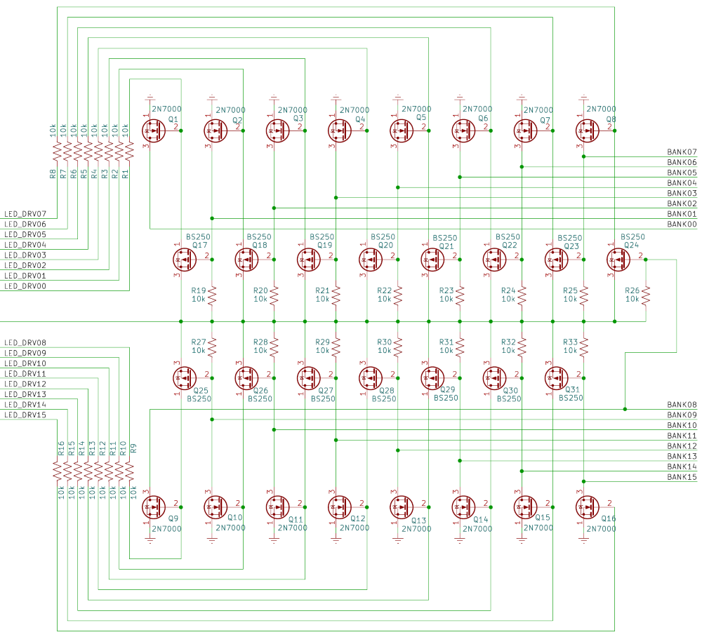
Figure 6. MOSFET display-driver matrix and cascaded MOSFET bridge.
7. PWM Brightness Control
A separate LM555-based PWM module was added to provide adjustable brightness without changing the LED resistor network. This PWM board modulates the decoder enable path at roughly 1 kHz. Because the enable path is active-low, the brightness behavior is inverted compared to the usual PWM interpretation: a longer LOW interval makes the display brighter, while a longer HIGH interval dims it. This also reduces average LED current and power consumption.
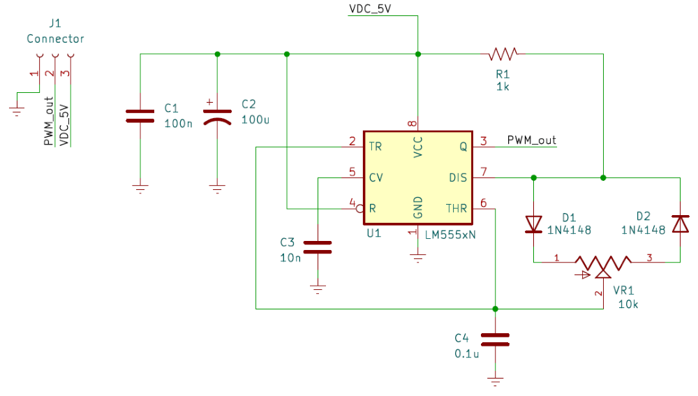
Figure 7. LM555-based PWM brightness-control board.
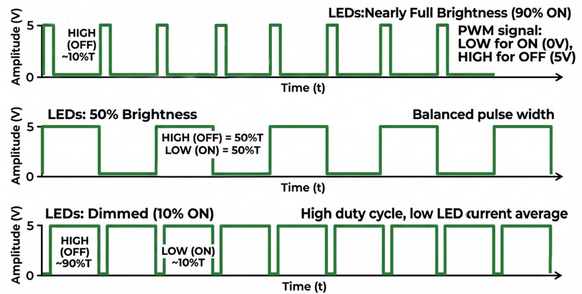
Figure 8. PWM timing diagram showing duty cycle versus visible display brightness.
Physical Description
1. The enclosure
A large portion of the project involved the mechanical design and physical integration of the electronics. The infinity mirror uses three circular ABS plastic panels spaced about 40 mm apart. The LED ring is mounted between the front and middle panels, while the rear panel holds the control electronics and user interface. The LED ring itself was 3D-printed to guarantee evenly spaced LED positions around the circular display.
The enclosure was designed so the front panel includes the microphone opening and mode switch, while the rear panel holds the DC input, main power switch, power indicator, and brightness adjustment control.
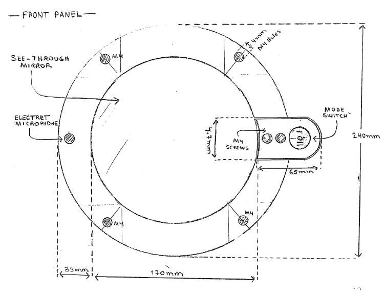
Figure 9. Front enclosure panel layout showing dimensions, microphone opening, mounting holes, and mode-switch.
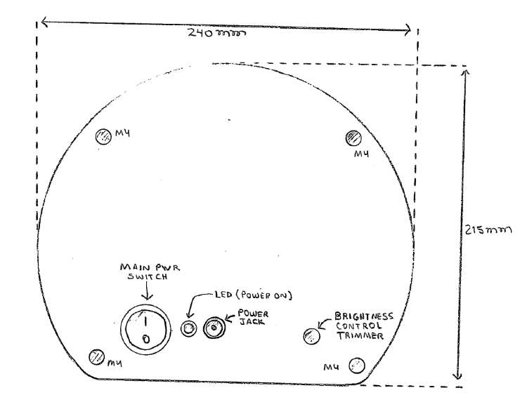
Figure 10. Rear enclosure panel layout showing DC input, main power switch, power indicator LED, and brightness-control location.
The LED ring has a 168 mm inner diameter, is 25 mm wide, and contains 54 evenly spaced 5 mm LED mounting holes. Two additional support frames were designed to hold the ring securely inside the enclosure and maintain proper alignment.
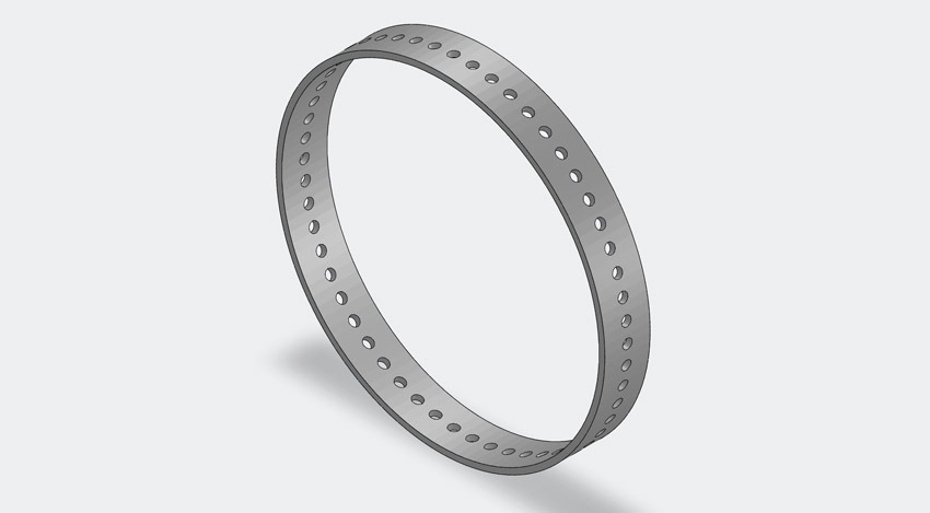
Figure 11. 3D-printed LED ring with 54 evenly spaced LED positions.
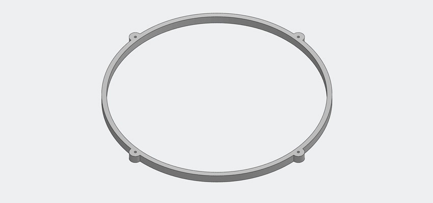
Figure 12. 3D-printed support frame used to align and secure the LED ring.
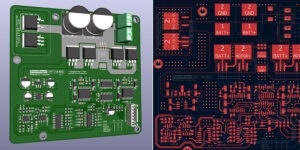
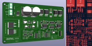
2. PCB Design & Layout
Version 2 uses a dedicated main control board and a separate PWM board. The main control board integrates the analog conditioning, ADC, logic decoding, and MOSFET interface circuitry. The PWM board was intentionally kept separate and connects to the main system through a 3-pin JST interface.
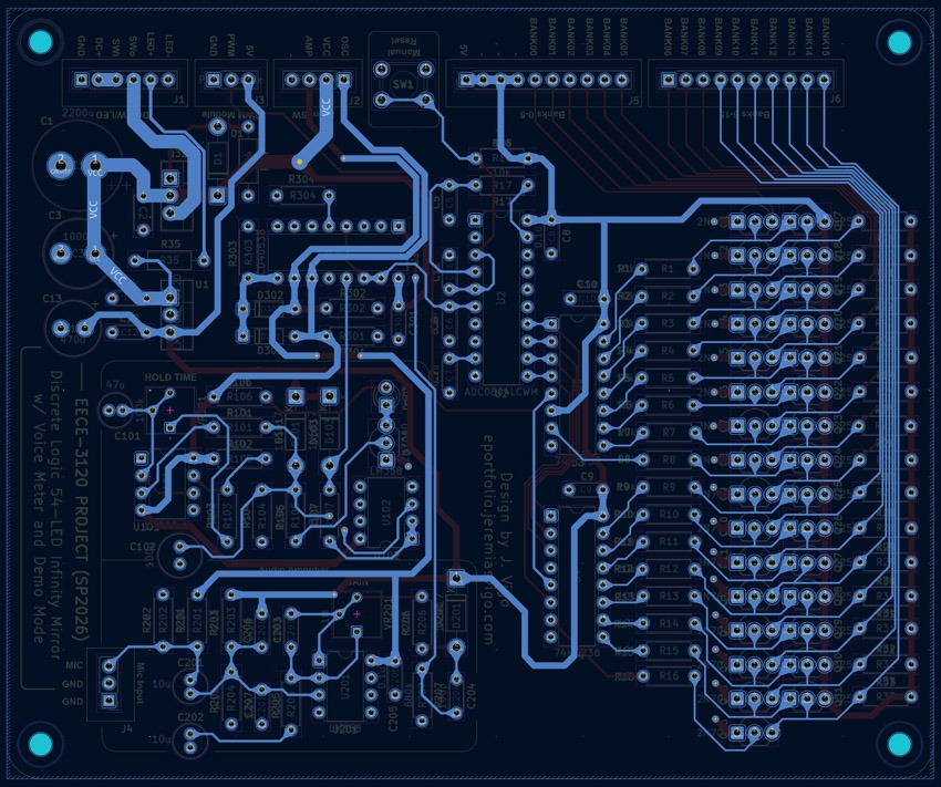
Figure 13. Main control board PCB layout, back copper traces.
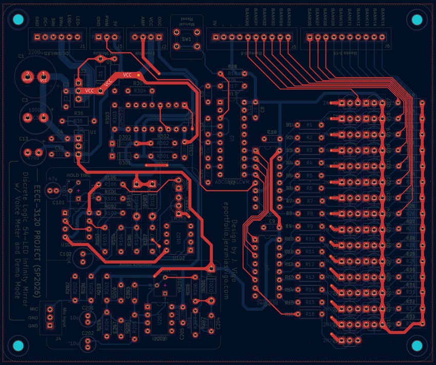
Figure 14. Main control board PCB layout, front copper traces.
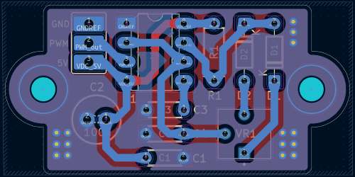
Figure 15. PWM control-board PCB layout with 3-pin connection to the main board.
The LED ring PCB is the main visual output element of the project. It contains 54 evenly spaced LED positions arranged around a circular structure. Electrically, it behaves like a radial bar meter: two bottom LEDs remain on as a fixed reference, and additional LEDs turn on in symmetric pairs as the input voltage increases. This behavior is controlled by the ADC and decoder stages, with the MOSFET bridge ensuring that lower banks remain active as higher banks are enabled.
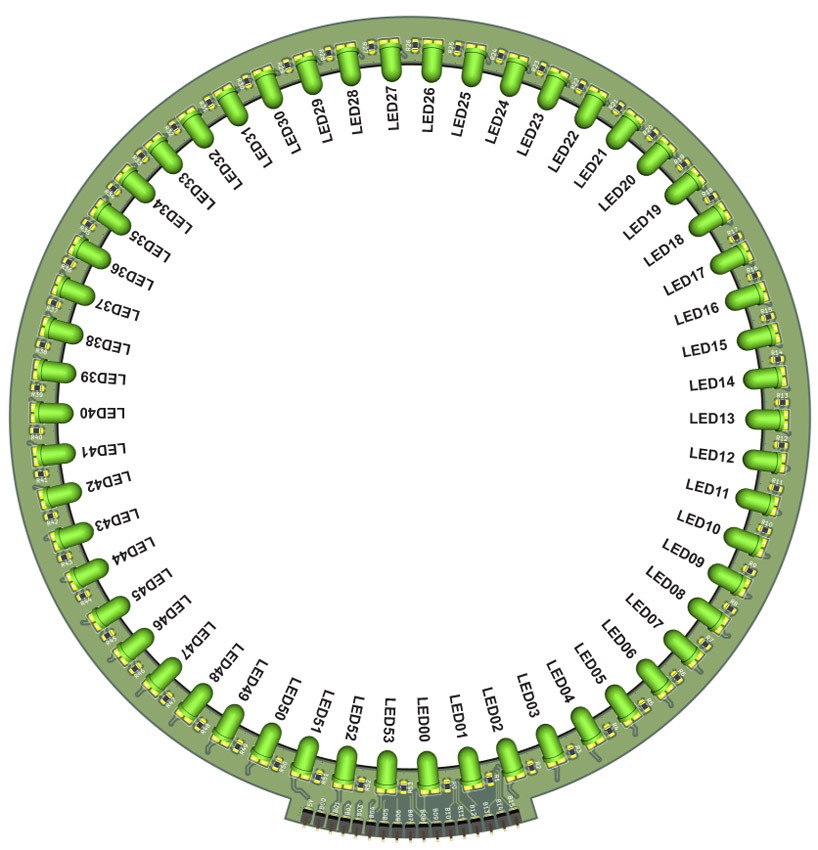
Figure 16. 54-LED ring PCB layout showing physical LED numbering and placement around the circular display.
Table 4. LED mapping and voltage thresholds
| Increment (V) | ADC MSB (D7-D4) | Active Stage | Left Side LEDs | Right Side LEDs | Total LEDs ON |
|---|---|---|---|---|---|
| 0.00V | 0000 | Idle | 53 | 00 | 2 |
| 0.31V | 0001 | Bank 1 | Previous + 52, 51 | Previous + 01, 02 | 6 |
| 0.63V | 0010 | Bank 2 | Previous + 50, 49 | Previous + 03, 04 | 10 |
| 0.94V | 0011 | Bank 3 | Previous + 48, 47 | Previous + 05, 06 | 14 |
| 1.25V | 0100 | Bank 4 | Previous + 46, 45 | Previous + 07, 08 | 18 |
| 1.57V | 0101 | Bank 5 | Previous + 44, 43 | Previous + 09, 10 | 22 |
| 1.88V | 0110 | Bank 6 | Previous + 42, 41 | Previous + 11, 12 | 26 |
| 2.20V | 0111 | Bank 7 | Previous + 40, 39 | Previous + 13, 14 | 30 |
| 2.51V | 1000 | Bank 8 | Previous + 38, 37 | Previous + 15, 16 | 34 |
| 2.82V | 1001 | Bank 9 | Previous + 36, 35 | Previous + 17, 18 | 38 |
| 3.14V | 1010 | Bank 10 | Previous + 34, 33 | Previous + 19, 20 | 42 |
| 3.45V | 1011 | Bank 11 | Previous + 32, 31 | Previous + 21, 22 | 46 |
| 3.76V | 1100 | Bank 12 | Previous + 30 | Previous + 23 | 48 |
| 4.08V | 1101 | Bank 13 | Previous + 29 | Previous + 24 | 50 |
| 4.39V | 1110 | Bank 14 | Previous + 28 | Previous + 25 | 52 |
| 4.71V+ | 1111 | Bank 15 | Previous + 27 | Previous + 26 | 54 |
Measurement Results
The completed system was tested to confirm that the major functional blocks behaved as intended and that all signal levels stayed within the ADC input range. The demo-mode oscillator was adjusted to operate between approximately 0.09 Hz and 0.21 Hz. That corresponds to a period range of about 11.1 s down to 4.76 s, which gives the LED pattern a slow and visually smooth motion across the display. The PWM board was measured at approximately 1 kHz, which is high enough to avoid visible flicker under normal viewing conditions. Since the PWM period is the reciprocal of frequency, the switching period is about 1 ms. The ADC threshold behavior also matched expectations. Since only the four MSBs are used, the 0–5 V input range is divided into 16 states, giving an ideal increment of:
ΔV=165V=0.3125V
This agrees with the measured threshold progression used by the display logic.
Current consumption was dominated by the LED display. Each LED uses a 1 kΩ series resistor, and with a 5 V supply and roughly 2.0 V forward drop, the current per LED is approximately:
At full scale, all 54 LEDs draw about:
The measured full-system current reached about 189 mA with PWM disabled and the display fully on in demo mode. With PWM enabled, the total current became adjustable from about 28 mA to 189 mA depending on brightness setting. This confirmed that the PWM module provided effective control over both light output and average current draw.
Table 5. Estimated Current Consumption Breakdown
| Functional Block | Component(s) | Current Contribution | Notes |
|---|---|---|---|
| Power Supply | LM7805 regulator | ~5 mA to 8 mA | Includes regulator quiescent current required to maintain the 5 V rail |
| Control Logic | ADC0804, 74HC238 (x2), CD4053 | ~4 mA to 7 mA | CMOS logic draws relatively little current; depends slightly on switching activity |
| Demo Oscillator | LM555 + LM358 buffer stage | ~3 mA to 6 mA | Includes the low-frequency oscillator and its output conditioning stage |
| Audio Stage | Electret microphone + LM358 amplifier | ~2 mA to 5 mA | Includes microphone bias and amplifier current; depends on gain adjustment |
| PWM Module | LM555 PWM circuit + indicator LED | ~4 mA to 8 mA | Used only when brightness control is enabled |
| MOSFET Matrix | 2N7000 and BS250 network | < 1 mA average | MOSFET gates are voltage-driven, so static current is negligible except during switching |
| LED Display | 54 LEDs @ ~3 mA each | ~162 mA max | Worst-case LED current when all LEDs are ON simultaneously |
| Total System Current (PWM ON) | All system active | Adjustable: ~28 mA to 189 mA | Average current depends on PWM duty cycle and resulting LED ON time |
| Total System Current (PWM OFF) | All system active, all LEDs ON | ~189 mA max | Worst-case full-brightness condition in demo mode with no PWM dimming applied |
Build Photos and Final Implementation
The finished Version 2 build shows the mechanical and electrical improvements made over the original version. The LED ring and support assembly give the mirror a more precise structure, while the enclosure panels and mounting hardware create a cleaner finished build.
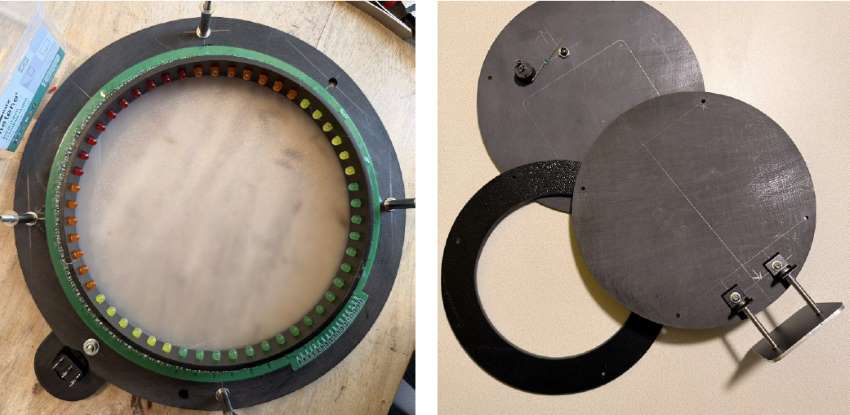
Figure A1. LED ring and support assembly (left) and enclosure panels with mounting hardware (right).
The completed system operates as both an aesthetic display and a functional hardware demonstration. The front view highlights the infinity mirror effect during operation, while the partially disassembled view shows the internal control electronics used to drive the display.
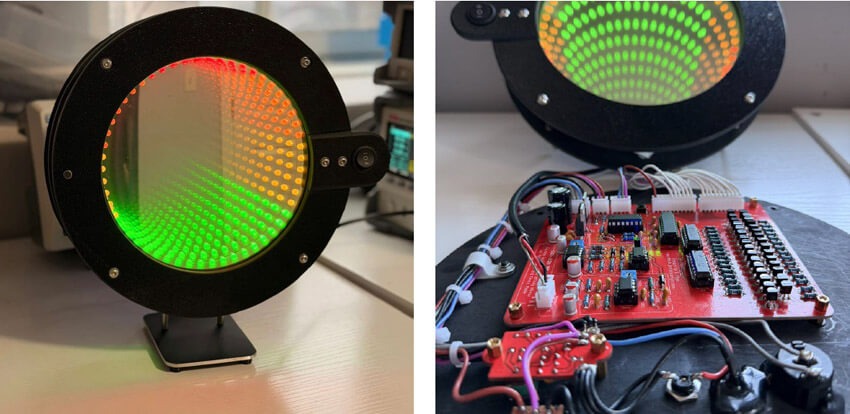
Figure A2. Completed infinity mirror during operation (left) and partially disassembled internal view (right).
The main control board integrates the analog, digital, and switching stages into a single custom PCB. Both the component side and solder side reflect the increased level of integration compared to the first version.
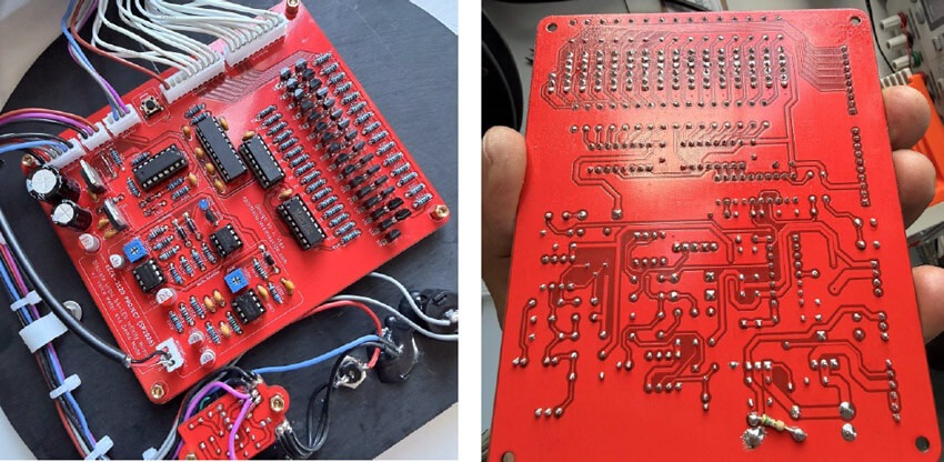
Figure A3. Main control board showing the front side (left) and soldered back side (right)
Close-up images of the control board show the low-frequency oscillator and audio amplifier sections. These are the two main analog front-end blocks that generate the signals used by the display.
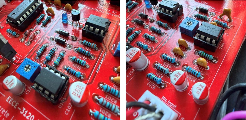
Figure A4. Close-up of the low-frequency oscillator section (left) and audio amplifier section (right).
Additional close-ups show the CD4053 input-selector stage, the ADC and decoder logic, and the MOSFET driver area. These blocks are responsible for selecting the signal source, converting it into digital levels, and expanding those levels into the final radial LED display.
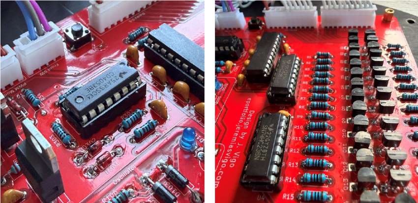
Figure A5. CD4053 input-selector stage (left) and ADC/decoder plus MOSFET driver section (right).
The power-entry and PWM sections are also shown in detail. These photographs highlight the reverse-polarity protection, 5V regulation stage, and the separate brightness-control board used to modulate the display.
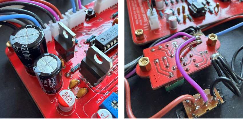
Figure A6. Reverse-polarity protection and 5V regulator section (left) and PWM brightness-control module (right).
Discussion
This project demonstrated that a functional infinity mirror can be built using only analog electronics, discrete logic, and MOSFET switching, without a microcontroller or programmable LEDs. One of the strongest parts of the design was the integration of both operating modes into a single system. Demo mode produced a slow and smooth sweep across the LEDs, while voice mode provided a sound-responsive radial meter. The CD4053 allowed both analog sources to share one ADC input in a stable and controlled way.
Another strong point was the display-driver architecture. By using only the four most significant ADC bits, the design divided the 0–5 V range into 16 levels while keeping the circuit manageable. The decoder and MOSFET bridge arrangement then expanded these levels into a cumulative LED pattern that behaved like a radial bar graph. The measured threshold mapping confirmed that the display followed the intended voltage steps and reached full scale at the highest level.
The PWM module was also an important improvement. It provided adjustable brightness and made it possible to reduce average system current without redesigning the resistor network. Version 2 further improved the project by reducing wiring, adding better PCB integration, and creating a cleaner final build overall.
Conclusion
The final design resulted in a fully functional 54-LED all-hardware infinity mirror capable of operating in both demo mode and voice-meter mode. The system successfully converted analog signals into a progressive LED display using an ADC0804, cascaded decoder stages, and a custom MOSFET driver matrix. A separate PWM board added adjustable brightness and current control, making the design more practical and efficient.
Measured results confirmed the expected oscillator behavior, ADC threshold mapping, PWM timing, and current consumption, with a worst-case full-system current of about 189 mA and a dimmed operating range down to about 28 mA. Overall, the project met its main goals and showed a strong combination of analog design, logic interfacing, PCB development, and physical system integration.
References
- Build Electronic Circuits. “555 PWM Circuit.”
- KiCad Design. Open-source EDA suite for schematic capture and PCB layout.
- JLCPCB. “PCB Prototype & PCB Fabrication Manufacturer.”
- Nexperia. 74HC238; 74HCT238 3-to-8 Line Decoder/Demultiplexer Datasheet.
- Next Electronics. “Multiple Waveform Generator Circuit Diagram.”
- TheoryCircuit. “Audio Amplifier Circuit Using LM358.”
- Texas Instruments. Industry-Standard Dual Operational Amplifiers (LM358 / LM358B datasheet).
- Texas Instruments. LM555 Timer Datasheet.
- Texas Instruments. CD405xB CMOS Analog Multiplexer or Demultiplexer with Logic-Level Conversion (CD4053B datasheet).
- Texas Instruments. ADC080x 8-Bit, µP-Compatible, Analog-to-Digital Converters (ADC0804 datasheet).
- Texas Instruments. LM340, LM7805 Fixed Voltage Regulators / LM7805 product documentation.