The analog “Code Breaker” circuit was built as part of my final design project for EECE 3110 Electronics I. It uses a combination of two resistors which determines the “secret code”. These resistors are between 1kΩ and 100kΩ and hidden by the Mastermind (in this case, me or the instructor). The job of the system is to verify the input resistances from two decade-boxes used by the Solver against the code, checking for both values and order. If the guessed combination is correct, the circuit will turn on a green LED; if it is not correct, a red LED will turn on to indicate the code did not match. The whole circuit was built using only analog components and concepts we have covered so far in this course.
I began this project by carefully selecting the correct components to make sure the circuit would operate within the desired expectations. Then an analytical approach was used to calculate the proper resistor values and reference voltages needed for the circuit to work as intended. Before getting to the hardware part, I simulated the circuit on Multisim, which helped confirm the expected behavior and fix any issues the circuit could present. Afterward, the circuit was built and tested on a breadboard, allowing hands-on adjustments and measurements. Once I verified that everything worked without a problem, I moved on to designing the PCB layout using Altium Designer. Using this step-by-step process helped me connect theory and real-world implementation into a complete engineering workflow.
COMPONENTS/PARTS LIST
Table 1 below shows a detailed list of all components and parts used in the project along with the contribution of each of them in the circuit.
Table 1. List of components used in the project.
| Reference | Component | Value | Function / Role |
| Power Rail | |||
| V1 | DC Source | 5 V | Main supply rail for entire circuit |
| S1 | SPST Switch | – | Turns system ON/OFF |
| C1 | Capacitor | 1 µF | Decouples VCC_5, stabilizes supply |
| Resistor Sensing Network | |||
| RG1 | Decade Box | 1–100kΩ | User-selected guess for resistor #1 |
| RG2 | Decade Box | 1–100kΩ | User-selected guess for resistor #2 |
| RC1 | Hidden Resistor | 20kΩ | CODE resistor #1 |
| RC2 | Hidden Resistor | 39kΩ | CODE resistor #2 |
| R1 | Resistor | 22kΩ | Forms voltage divider with RG1 (VG1) |
| R2 | Resistor | 47kΩ | Forms voltage divider with RG2 (VG2) |
| R3 | Resistor | 3.9kΩ | Generates high threshold (VREF1_H) |
| R4 | Resistor | 22kΩ | Generates low threshold (VREF1_L) |
| R5 | Resistor | 6.8kΩ | Generates high threshold (VREF2_H) |
| R6 | Resistor | 47kΩ | Generates low threshold (VREF2_L) |
| Window Comparator (Channel 1) | |||
| U1A | LM358 Op-Amp | – | Upper threshold comparator (VG1 vs VREF1_H) |
| U1B | LM358 Op-Amp | – | Lower threshold comparator (VG1 vs VREF1_L) |
| D1 | 1N5817 Diode | Schottky | Combines comparator outputs into logic node |
| D2 | 1N5817 Diode | Schottky | Combines comparator outputs into logic node |
| Window Comparator (Channel 2) | |||
| U2A | LM358 Op-Amp | – | Upper threshold comparator (VG2 vs VREF2_H) |
| U2B | LM358 Op-Amp | – | Lower threshold comparator (VG2 vs VREF2_L) |
| D3 | 1N5817 Diode | Schottky | Combines comparator outputs into logic node |
| D4 | 1N5817 Diode | Schottky | Combines comparator outputs into logic node |
| Comparator Output Logic | |||
| R7 | Resistor | 1kΩ | Pull-up for diode OR logic node |
| R8 | Resistor | 1kΩ | Output series resistor to VCOMP |
| Q1 | 2N7000 MOSFET | N-channel | Drives PASS LED when VCOMP ≈ HIGH |
| PASS Indicator (Green) | |||
| PASS LED | LED (Green) | – | Indicates correct code |
| R9 | Resistor | 470Ω | PASS LED current limiter |
| FAIL Indicator (Blue) | |||
| Q2 | 2N7000 MOSFET | N-channel | Drives FAIL LED when VCOMP ≈ LOW |
| FAIL LED | LED (Blue) | – | Indicates incorrect code |
| R10 | Resistor | 470Ω | FAIL LED current limiter |
DESIGN OVERVIEW
The circuit converts both guess and code resistors into a specific voltage through a set of resistor dividers. The hidden code resistors generate two reference threshold levels (VREF_H and VREF_L) for each channel, while the guess resistors generate two voltages (VG1 and VG2). These guess voltages are connected to a pair of LM358 comparators configured as window comparators. Each comparator pair checks if a guess voltage is between the upper and lower threshold (defined by the hidden code resistors). If it falls outside the window, that channel will fail immediately and the red LED will turn on. Otherwise, the green LED will light up to show that the code combination matches.
The outputs of the comparators are combined using a diode-AND logic network. In this case, all four comparators (two per channel) must agree before the circuit produces a “PASS” result. This only happens when both guess resistance match the hidden code—both in value and position—producing a high logic output (VCOMP). This logic signal directly (and indirectly) drives two MOSFETs: Q1 (controlling the green LED) and Q2 (controlling the red LED). Together, each stage of the circuit forms a complete analog system that checks a two-resistor code, without the use of microcontroller, while remaining stable and simple to operate.
The circuit was designed and tested using Multisim prior to the breadboard assembling and PCB design. Figure 1 shows the full schematic of the circuit (excluding the power supply block). It shows the three main stages and the voltages on specific parts of the circuit—measured while the simulation was running and the circuit was at the “PASS” mode.
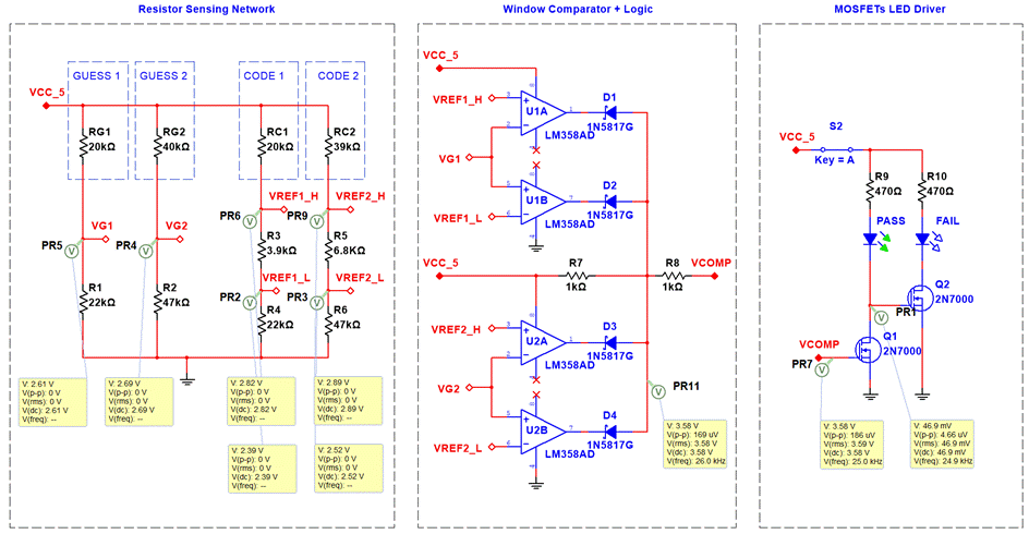
Figure 1. Full schematic of the Code Breaker Circuit (excluding the power supply).
- Power Supply/Switch
Originally, the idea was to use two different voltage rails to power the circuit. However, I decided to keep it simple and use a single low-voltage rail instead. This makes the design more breadboard-friendly and safer. This 5V simple rail (Figure 2) uses an external voltage source and powers every stage of the circuit (sensing network, comparators, and LED drivers).
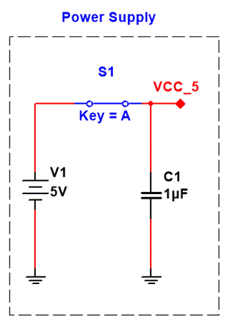
Figure 2. Schematic of the power supply.
- Resistor Sensing Network
The resistor sensing block shown in Figure 3 is the part responsible for converting the four resistances (RG1, RG2, RC1, and RC2) into voltages (VG1, VG2, VREF1, and VREF2).
- Guess channels (VG1 and VG2)
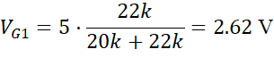
Each guess resistor forms a voltage divider with a fixed resistor connected to ground. The node between the two resistors is the sensed voltage. For example, using RG1=20kΩ and R1=22kΩ, will produce:
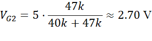
And for RG2=40kΩ and R2=47kΩ we get:
Because R1 and R2 are fixed value resistors, the voltages we just calculated only depend on the guessed resistance values (from the decade box), so that each resistor value results in a voltage (VG) between 0V and 5V. We can clearly see the behavior of each resistor in the resistor sensing network (Figure 3) and how the simulated voltages on each node closely support the theoretical results.
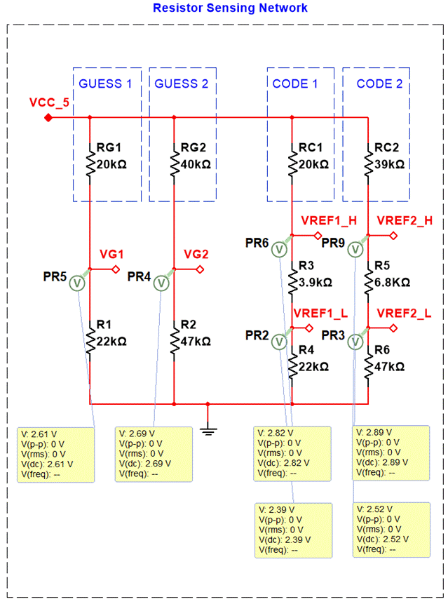
Figure 3. Schematic of the Resistor Sensing Network block.
- Code channels and reference windows (VREF_H and VREF_L)
Each code resistor is part of a three-resistor ladder with two fixed resistors to generate top and bottom window thresholds:
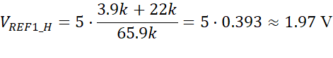
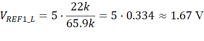
- Channel 1: RC1=20kΩ, R3=3.9kΩ, R4=22kΩ
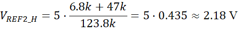
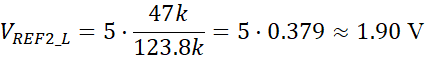
- Channel 2: RC2=39kΩ, R5=6.8kΩ, R6=47kΩ
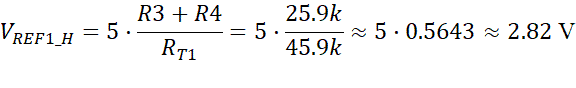
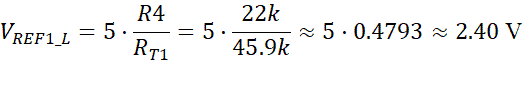
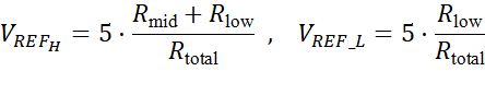
For channel 1, the upper (VREF1_H) and the lower (VREF1_L) threshold voltage are calculated simply using the voltage divider equation. Considering the sum of all series resistance (RT1) is 45.9kΩ, then the upper and lower thresholds are:
The same method is used to find the thresholds (VREF2_H and VREF2_L) for channel 2. Here, the sum of the total series resistance (RT2) is 92.8kΩ. This gives us the following upper and lower thresholds:
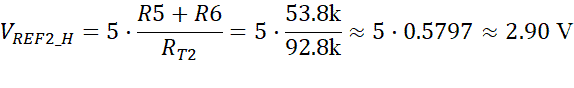
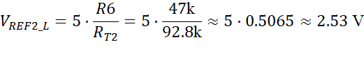
These reference voltages (VREF_H and VREF_L) define a fixed window that corresponds to the correct code resistor values. As long as the Solver uses the same hidden resistors, the window stays constant.
- Window comparator + logic circuit
This stage uses two LM358 op-amps per channel (U1A/U1B and U2A/U2B) configured as window comparators, and Schottky diodes to combine the two-channel outputs into a single logic node, using an “AND” style configuration.
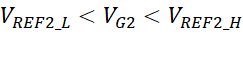
The outputs from the comparators (U1 and U2) pass through diodes D1, D2, D3, and D4 (cathodes at op-amp outputs, anodes tied together at the logic node). When either one of the comparators outputs low, the diode that is connected to its output clamps, pulling the logic node low. On the other hand, if the output is high, the diode will most likely not conduct, and the logic node will remain high—as long as all comparators’ outputs are also high. The logical condition for channel 1 to output high can be described as:
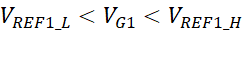
and
The pullup resistor (R7) keeps the logic node high all times unless one of the diodes is clamped to a low output. R8 connects the logic output to the next stage. The schematic block of the window comparator and the logic output is shown in Figure 4.
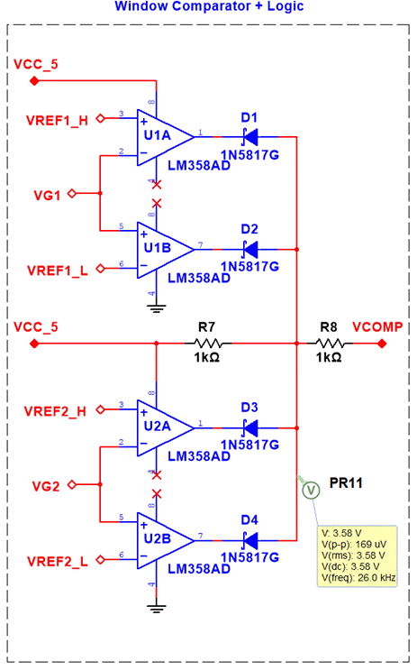
Figure 4. Schematic of the Window Comparator + Logic block
Table 2 is the truth-table view of this stage showing input vs output response to each input VG. VCOMP is the node coming out of the logic network after R8. Note (in Table 1) that VCOMP is only high when both VG1 and VG2 are inside the threshold/window (IN RANGE) determined by the comparator.
Table 2. Truth table of Stage 3 (Window Comparator + Logic).
| Case | VG1 vs Window 1 | VG2 vs Window 2 | VCOMP | Result |
| 1 | IN RANGE | IN RANGE | HIGH (~3.6 V) | PASS |
| 2 | OUT OF RANGE | IN RANGE | LOW | FAIL (wrong for position 1) |
| 3 | IN RANGE | OUT OF RANGE | LOW | FAIL (wrong for position 2) |
| 4 | OUT OF RANGE | OUT OF RANGE | LOW | FAIL (both wrong) |
Figures 5 and 6 are the transfer curves showing the window in which the LED are either on or off. The graph on Figure 5 shows the plot corresponding to the behavior of the output of the first comparator (U1) in response to each input level. Figure 6 shows the same behavior for the second comparator (U2). Both graphs compare the ANDed output (VCOMP) as a response of its inputs (VG1 and VG2).
For my design, I decided that a window of about ~ 0.4V would be more than enough to compensate for any variation in resistance the system could have. But this can be adjusted by changing the values of R3, R4, R5, and R6 at the resistor sensing circuit network.
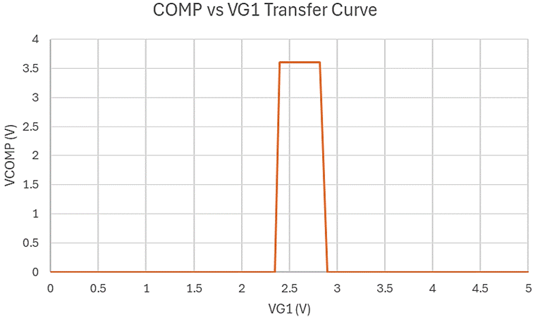
Figure 5. Graph of the comparator window for COMP vs VG1.
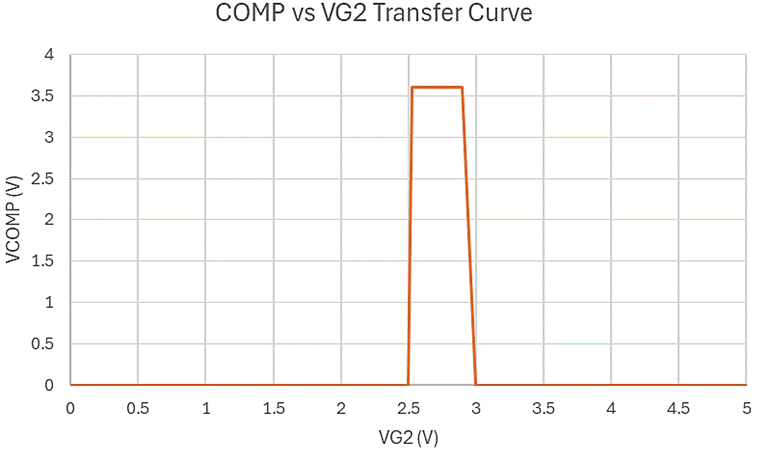
Figure 6. Graph of the comparator window for COMP vs VG2.
- MOSFET LEDs driver
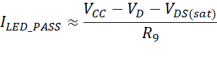
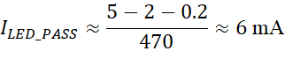
The job of this block is to convert the logic voltage VCOMP into visible PASS/FAIL indications using two N-channel MOSFETs (2N7000) and separate LED branches. Figure 7 shows the schematic of the MOSFET LED driver stage. Notice in the simulated levels, when VCOMP is HIGH (~3.6 V), Q1 turns ON, its drain–source channel saturates, and current flows. This gives us about 6 mA through “PASS” LED (using VD=2V and VDS(SAT)=0.2V):
On the other hand, when VCOMP is LOW, VGS(Q1) is ~0V and Q1 is off. This makes the PASS LED current ~0A and VGS(Q2) around 5V (VCC_5), turning Q2 and “FAIL” LED on.
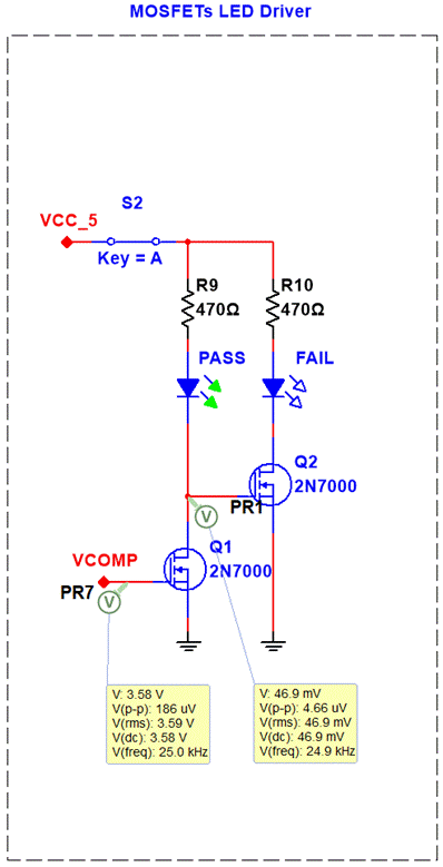
Figure 7. Schematic of the MOSFET LED driver stage (PASS/FAIL outputs).
Table 3 shows the exact operation of this stage given different input conditions.
Table 3. PASS/FAIL Logic Behavior (Q1 & Q2 Operation)
| Condition | Q1 State | Q2 Gate Voltage | PASS LED | FAIL LED | Result |
| Code is Correct | ON | Pulled LOW (near 0V) | ON | OFF | PASS |
| Code is Wrong | OFF | Pulled HIGH through PASS LED resistor | OFF | ON | FAIL |
- Physical implementation: Breadboard and PCB design
The design involved assembling and testing the circuit on a breadboard (Figure 8). This allowed me to test everything in a real environment before the PCB design. The breadboard implementation confirmed that each stage of the circuit operated correctly and that the LED indicators behaved exactly as expected—as different code and guess values were applied.
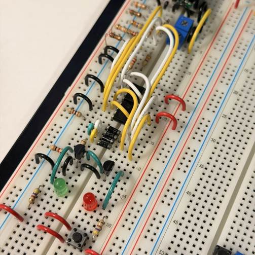
Figure 8. Breadboard implementation of the Circuit.
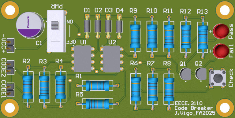
After testing the breadboard circuit, I created a PCB layout using Altium Designer (this was my first time using this software). I try keeping the sensing block and LED driver section separate to minimize noise. I also labeled all connectors and major components to better reflect the circuit’s purpose and kept traces around the comparator and reference block shorter for stability. Figure 9 shows the screenshot of the full PCB layout from Altium Designer.
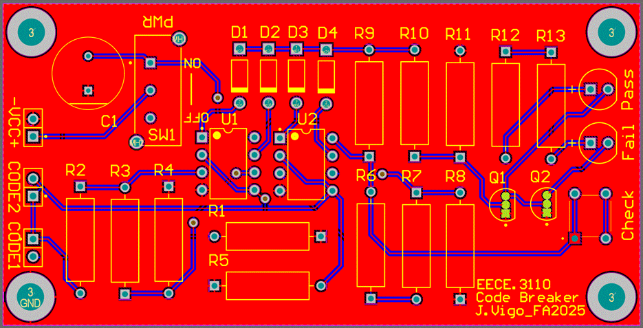
Figure 9. PCB layout from Altium Designer.
The render in Figure 10 shows the 3D simulation with all components, including the LM358 ICs, diodes, resistors, MOSFETs, and LEDs. I did my best positioning CODE1, CODE2, and Power connectors for easier access and placed the PASS/FAIL LEDs next to the check button for better visualizations of results.
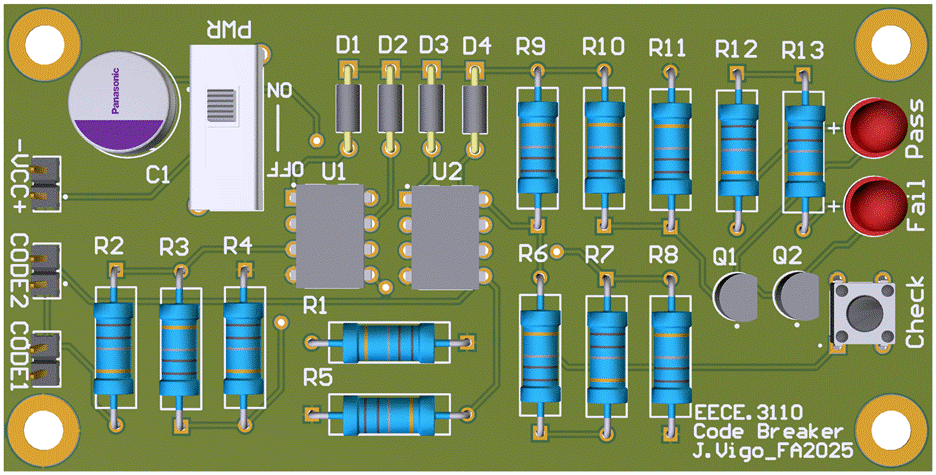
Figure 10. 3D simulation from Altium Designer.
The fabrication files, including Gerber and drill files were also exported after the completion of the PCB and will be submitted as part of this project.
- Design flexibility
One of the major advantages of my design is that the “CODE” can be changed at any time simply by replacing the two hidden CODE resistors (RC1 and RC2). No recalibration or modification of the sensing network or comparator circuit is needed. This is an intentional behavior of the design.
The reason this works is because each CODE resistor is part of a three-resistor ladder network:
- Channel 1 ladder: RC1 – R3 – R4
- Channel 2 ladder: RC2 – R5 – R6
In each ladder, the CODE resistor is part of the voltage divider that makes the upper and lower window thresholds:
Because RCODE is in the denominator, changing its value automatically shifts both the upper and lower thresholds to a new level. The comparator window then adjusts to the new resistor value with no other adjustments needed.To test this flexibility, I replaced the original code resistors as follows:
- RC1 from 20kΩ to 40kΩ
- RC2 from 40kΩ to 70kΩ
As a result of this change, the new upper and lower threshold became:
- For channel 1:
- For channel 2:
I observed that the window was slightly narrowed compared to the original values, but this did not affect the overall function of the circuit.
- Electrical Specifications
The circuit was designed to operate at 5V—can even be powered by a USB charger without a problem. The LM358, for example, can handle anything from 3V up to 32V, so using only 5V gives us a good safety margin. At this voltage, all sensing and reference voltages (VG1, VG2, VREF_L, VREF_H) stay inside the LM358’s input range. The MOSFETs and LEDs also work fine at 5V as they are limited to around 6 mA by the 470 Ω resistors. In addition, the circuit was designed so that the PASS and FAIL LEDs never turn on at the same time, so the power supply is never overloaded. Table 4 shows the complete electrical specifications of the circuit.
Table 4. Electrical Specifications of the Code Checker Circuit
| Parameter | Typical Values | Min | Max (Safe) |
| Supply voltage (single rail) | 5V | 4.5V | 32V (LM358 max) |
| Quiescent current (approx.) | 3–5 mA | – | – |
| PASS LED current | ≈ 6 mA | ≈ 4 mA | 10 mA |
| FAIL LED current | ≈ 6 mA | ≈ 4 mA | 10 mA |
| Total LED current | ≈ 6 mA | – | 10 mA |
| Comparator input common-mode range | 0–3.5V | 0V | VCC – 1.5V (typ.) |
| Temperature | 25 °C | 0 °C | 70 °C |
DISCUSSION
This design was able to combine multiple concepts—such as voltage dividers, comparator behavior, diode logic, and MOSFET switching—to work together and create a complete functional system. Each stage behaved as predicted, and the idea to implement the window comparator was both an accurate and flexible method to get this to work. One of the most important observations from testing the circuit was how stable the reference windows were. Even small changes in the guessed resistance produced noticeable changes in VG1 and VG2, which makes it easy for the comparators to detect correct versus incorrect values—within about 5% error range, which is perfect when we are dealing with 5% tolerance resistors.
The diode-AND logic also worked very as I had expected. Because the diodes isolate each comparator output, a single low output immediately makes VCOMP low, which is exactly what we want for a PASS/FAIL system. The MOSFET driver stage reflects this behavior into a visual result using LEDs. The breadboard prototype and the measured voltage values matched closely with simulation results. Finally, transferring the design to a PCB gave the circuit a professional look and made it more compact and easier to use.
CONCLUSION
Overall, the Code Breaker circuit successfully met all project’s expectations by using analog only components to generate and check on a combination of two-resistor code. The LM358 comparators, the resistor network, and diode logic worked together to form a simple, but effective decision-making system, while the MOSFET drivers provided straightforward PASS/FAIL feedback. The circuit was also found to be flexible enough such that changing the hidden code only requires swapping the two CODE resistors, and the reference window will automatically update without any redesign. Both the breadboard version and PCB implementation performed the way it was designed to, showing that a fully analog circuit can be safely used in a stable and intuitive code-checking system.
Online References
- Analog Zoo. (2023). Window comparator circuit demonstration [Video]. YouTube.
https://youtu.be/anEwM1IKlWk?si=iyYvDrQ2EBaL0dWb - ElectronZap. (n.d.). Window comparator tutorial and circuit examples.
https://electronzap.com/window-comparator/ - Texas Instruments. (2016). LM358 Low-Power Dual Operational Amplifier (Datasheet).
https://www.ti.com/lit/ds/symlink/lm358.pdf?ts=1764441820164 - Microchip Technology. (2023). 2N7000 – N-Channel Enhancement-Mode Vertical DMOS FET (Datasheet).
https://ww1.microchip.com/downloads/en/devicedoc/2n7000-n-channel-enhancement-mode-vertical-dmos-fet-data-sheet-20005695a.pdf