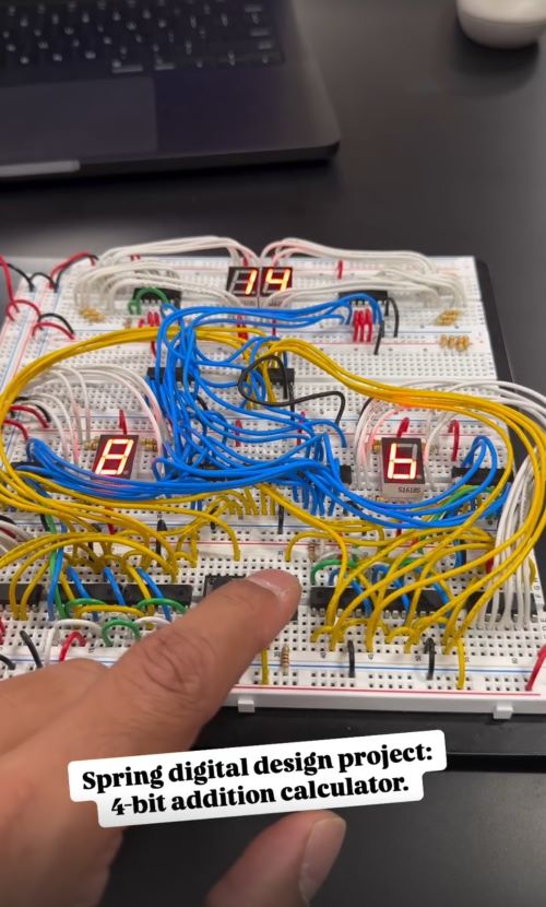
The goal of this project was to design a digital 4-bit summing calculator that could add two single-digit decimal numbers ranging from 0 to 9. The result is displayed using two 7-segment displays, which output the sum from 0 to 18 (e.g., 9 + 9). This basic design project takes advantage of digital logic components such as flip-flops, full-adders, display decoders, AND/OR gates, Schmitt Trigger inverters and other passive components to achieve the desired outcome.
SYSTEM OVERVIEW
The following are some of the major components used in the project, as well as a brief description on how they operate.
- Asynchronous Counters
The project contains two asynchronous counters, counter #1 and counter #2. Each of them uses four JK flip-flops (two 74LS76 chips) and can handle up to 4-bit, giving them the ability to count from 0 to 15. However, for the purpose of this project, they were designed to count only from 0 to 9 (0000 to 1001) and then restart counting after that. To accomplish this, the logic circuit —a combination of AND and NOT gate (inverter)— shown in Figure 1 was created to trigger the counter’s reset pins high when it reaches the value of 10 (1010).
Both counters increment on the falling edge of a button press and the debouncing is made by a 74LS14 (Hex Inverter with Schmitt Trigger) along with a 10uF capacitor as seen on Figure 1. The input of the inverter connected to the switch has a pull-down resistor of 1KΩ. The pull-down resistor ensures that the input of the inverter stays low when the button is not pressed. This will prevent the clock input of the JK flip-flop to be floating. As we can notice on the schematic below, the inputs J and K on each flip-flop are tied together to enable the trigger mode every time a clock signal is received. The output of each flip-flop is connected to its corresponding input on the 74LS47 (7-segment decoder), which connects to a single-digit 7-segment display.
Figure 1. Schematic highlighting both counter #1 and counter #2
- Full Adder Blocks
The outputs of both counter #1 and counter #2 are connected to inputs A and B respectively of the first full adder (74LS283). The full adder calculates the binary sum of the two counters’ output, outputting a 4-bit result plus a carry-out (for sums over 15). The output sum of the full adder is then connected to input A of a second adder, as seen on the schematic on Figure 2. The second adder was implemented as part of a problem solving that we were having.
At first, the idea was to have a single adder and have its output displayed in a 7-segment display. However, everytime the sum value exceeded 9 (1001) the display would show hex values instead of decimals. To correct this problem, the logic circuit network shown on Figure 2 was implemented between the adder and the display decoder. The circuit works by resetting the LSB display back to 0 (0000) everytime it reaches the value of 10 (1010) and incrementing the MSB display by 1 (refer to point 3 for more details). Although it seems like everything worked at first, we found another problem with this configuration. The system would only display results from 0 to 15 which would limit the ability to display the sums of higher values. For example, adding 8 + 8 would result in 0 instead of 16, adding 9 + 9 would result in 2 instead of 18, and so on.
Figure 2. Schematic highlighting the two full-adders.
In order to address this issue, we needed the output of the LSB display (right) to be incremented by 6 (0110) for certain output values. Therefore, a second full adder and an AND gate were implemented to the circuit. The output of the first full adder was then tied to input A of the second full adder, while input B (of the second full adder) was fed by a constant value of 6 at sum outputs greater than 15. The binary value of 0110 was produced by grounding pins 7 and 11 of the second full adder and connecting pins 2 and 15 to the output of the new AND gate. The inputs of the AND gate were then connected to VCC and the carry out of the first full adder, respectively. This would ensure that the increment of 6 would only apply for sums greater than 15.
- BCD Correction Logic Circuit
One of the first problem-solving steps of the design was to figure out a way to reset the LSB display back to 0 (0000) and increment the MSB display by 1 once the sum reached the value of 10 (1010). In order to accomplish such behavior we needed to create a multiplexer circuit that would act as a multiplexer between the full adders’ output and the input of the 7-segment decoder.
Figure 3. Schematic highlighting the logic circuit used as display multiplexer.
The highlighted section on Figure 3 shows the logic circuit that was created to achieve the desired behavior. The calculations below were used to determine the boolean expressions for each input/output bit prior to designing the new logic circuit. Notice that inputs B, C and D were changed into a new output, but the least significant bit, A, remained the same. This explains why bit A connects directly to channel A of the 7-segment decoder, while bits B, C and D have to pass through the newly designed logic circuit.
| Truth table |
| A = A | B = D’B + DCB’ |
| C = D’C + CB | D = DC’B’ |
- Seven-segment Display Decoder
The project implements four 7-segment display decoders (74LS47). Two of them are used to drive the single digits display at the output of each counter. The other two are used to drive the display for the sum. These decoders are responsible to convert the BCD values into voltages that are necessary to power the LEDs at each 7-segment display. The pin configuration of these chips are very straight forward. Pin A receives the first bit from the second full adder’s output. Pin B, C and D receive the second, third, and fourth bit from the multiplexer circuit from Figure 3, respectively. The output pins (a to g) connect to the 7-segment display, through load resistors of 330Ω, to its corresponding inputs (A to G).
Figure 4. Wiring of the 7-segment decoder and the display.
- Logic Gates
Among all the major components noted above, the project also uses other basic but indispensable components, which includes different types of logic gates, in order to operate properly. Here are some of them:
- AND gates (74LS08) – The project uses a total of three 74LS08’s chips. Each one of these chips contain four AND gates. The pin configuration and technical specification of the chip is attached to Appendix B.
- OR gates (74LS32) – There is only one 74LS32’s chip being used in this project. Similar to the AND gate, the chip contains four OR gates that can be used independently. The pin configuration and technical specification of the chip is attached to Appendix B.
- Schmitt Trigger inverters (74LS14) – There are two 74LS14’s chips being used in this project. They are mainly used to invert an input signal relative to the output. It generates a boolean expression of y = y’. They are also used for debouncing the button signals along with a 10uF capacitor. Each one of these chips integrates a total of six inverters. The pin configuration and technical specification of the chip is attached to Appendix B.
DATA AND RESULTS
Table 1 contains some important information about the electrical specifications of the calculator, such as supply voltage and current consumption. Although some components used in the design can handle higher supply voltages, the maximum supply voltage supported by the calculator itself is 5.25V. This value is based on the maximum supply voltage of some ICs, such as the 74LS08 and 74LS32, according to their datasheets.
The operating current consumption of the calculator was calculated using a digital multimeter. The maximum value was determined when the greatest number of LEDs (on the 7-segment displays) were lit simultaneously. For example, the maximum current was measured when counters #1 and #2 had an output of 8 (1000) and the sum was 16. The minimum value, however, was measured when both counters had the value 1 and the sum was 2.
Table 1. Electrical specifications of the calculator
| Electrical specifications | ||
| Operating voltage | Maximum supply voltage | 5.25V |
| Minimum voltage | 4.25V | |
| Operating current | Maximum current draw | 250mA |
| Minimum current draw | 160mA | |
CONCLUSION
In this project, we successfully built a simple 4-bit binary calculator that can calculate values up to 18 using the addition method. We were able to complete the project using a single 4-block breadboard provided by the professor. For our design, we used two asynchronous counter blocks made of JK flip-flops and two full adders to sum the output of the counters. In addition, we used four 7-segment displays to display the results of the counters and the final sum.
Although we were able to simulate the circuit before actually building it, this did not prevent the problems we encountered along the way. There were a lot of troubleshooting involved before we finally completed the project, which surely contributed to sharpen our understanding about digital logic circuits. One of the main and most challenging problems we faced was when we had to modify a large portion of the already built circuit to increment the display by 6 when the sum reached the value of 16. The fact that we were able to create a correction logic circuit specifically to solve this problem demonstrates a practical approach to digital circuit design and helped us develop the problem-solving skills that we needed.

References
KiCad EDA. Schematic Capture & PCB Design Software, KiCad Developers Team, 1992-2024, https://www.kicad.org/
Multisim Online Software. Web-base electrical simulation software. National Instruments Corp ©, 2025, https://www.multisim.com/
Tocci, Ronald. et al. Digital Systems, 12th edition, published by Pearson Education © 2017, http://www.pearsonglobaleditions.com/


