Project Overview
The controller is designed for applications such as RC vehicles, rovers, small trains, mobile robots, and future elevator-style prototypes where regenerative energy recovery could be useful. The design is based around a TL494 PWM controller, an IRF3205 MOSFET H-bridge, IR2110S high-side/low-side gate drivers, and digital mode-selection logic.
The system supports five operating modes:
- Coast
- Forward drive
- Reverse drive
- Forward regenerative braking
- Reverse regenerative braking
The current version is designed for a 12 V / 5 A operating range and includes several protection features to improve reliability during motor startup, braking, and regenerative operation.
Main Features
- TL494-based PWM speed control
- Full MOSFET H-bridge for bidirectional DC motor control
- IR2110S high-side/low-side MOSFET gate drivers
- Forward, reverse, coast, forward-regen brake, and reverse-regen brake modes
- PWM-controlled regenerative braking
- 0.05 Ω current-sense resistor for current limiting
- 5 A current-limit feedback into the TL494
- CD4053 analog switching for bidirectional motor-voltage feedback
- Dual SN74153 multiplexers for digital mode selection
- Battery/DC-bus overvoltage protection during regeneration
- MOSFET-controlled dump-load circuit using a 20 Ω / 35 W resistor
- TVS diode and dual 2200 µF bulk capacitors for DC-bus protection
- Local H-bridge decoupling capacitors for high-frequency switching stability
- Custom PCB layout with large copper areas for high-current routing and heat spreading
Circuit Breakdown
1. Power Supply and DC-Bus Section
The power supply section receives the main battery input and generates the voltages needed by the controller. The main motor supply is connected to the BATT+ / VCC rail, which feeds the H-bridge power stage and the rest of the circuit.
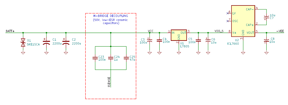
The DC bus includes:
- A TVS diode across the battery input for transient spike suppression
- Two 2200 µF bulk capacitors to support motor startup current and reduce bus ripple
- A 7805 regulator to generate the 5 V logic supply
- An ICL7660 charge pump to generate a small negative voltage rail for the LF398 sample-and-hold circuit
- Additional 100 nF and 10 µF decoupling capacitors around the regulator and charge pump
One important update in this revision was the addition of local H-bridge decoupling capacitors between the motor supply rail and the high-current return node. These capacitors are placed closer to the MOSFET bridge than the large electrolytic capacitors. Their purpose is to handle fast switching transients that the larger bulk capacitors cannot respond to as quickly.
This helps reduce high-frequency voltage spikes, improves switching stability, and lowers stress on the MOSFETs and gate-driver section.
2. Control and Feedback Section
The control section is built around the TL494 PWM controller. The TL494 generates the PWM signal used to control motor speed. The PWM frequency is set by the RT/CT timing network, and the output is routed to the digital logic section that determines which MOSFETs receive the PWM signal.
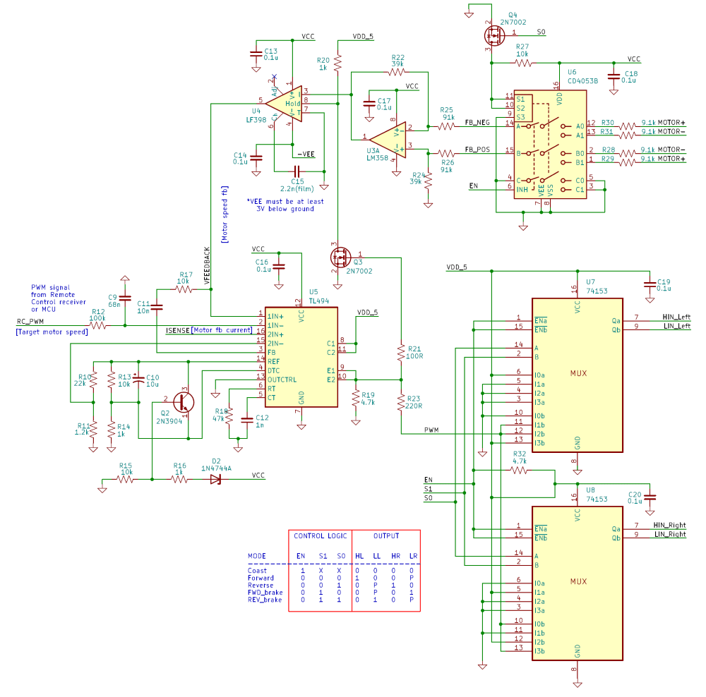
The control circuit uses two main feedback paths:
- Speed / Motor-Voltage Feedback
The motor-voltage feedback circuit scales the voltage across the motor before sending it to the TL494 feedback input. The differential amplifier gain is set by the resistor ratio:
Av=Rf/Rin
Using Rf=39kΩ:
Rin=91kΩ+9.1kΩ=100.1kΩ
Av=39kΩ/100.1kΩ ≈0.39
For a 12 V motor voltage:
Vfeedback = Av×Vmotor
feedback = 0.39×12V
feedback ≈ 4.68V
Therefore, a 12 V motor voltage is scaled down to approximately 4.7 V, which keeps the feedback signal within the TL494’s 0–5 V control range.
- Current Feedback
The motor current is monitored using a 0.05 Ω current-sense resistor in the low-side return path. The current limit is set to approximately 5 A.
V=I×R
V=5A×0.05Ω
V=0.25V
Therefore, when the voltage across the shunt resistor reaches approximately 0.25V, the controller detects that the motor current has reached the 5A current limit. At this point, the TL494 reduces the PWM duty cycle to help protect the power stage.
3. H-Bridge Power Stage
The power stage uses four IRF3205 N-channel MOSFETs arranged as a full H-bridge. This allows the motor to be driven in both directions.
The high-side and low-side MOSFETs are driven by two IR2110S gate-driver ICs. These drivers are necessary because the TL494 and digital logic cannot directly drive the MOSFET gates, especially the high-side MOSFETs. The IR2110S drivers provide the required high-side/low-side gate-drive signals and use bootstrap capacitors for the high-side drive.
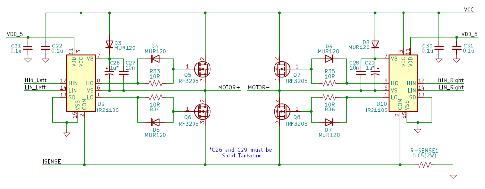
The H-bridge supports the following output states:
| Mode | HIN_L | LIN_L | HIN_R | LIN_R |
|---|---|---|---|---|
| Coast | 0 | 0 | 0 | 0 |
| Forward | 1 | 0 | 0 | PWM |
| Reverse | 0 | PWM | 1 | 0 |
| Forward regen brake | 0 | PWM | 0 | 1 |
| Reverse regen brake | 0 | 1 | 0 | PWM |
The logic signals are generated using dual SN74153 multiplexers. These multiplexers route the PWM and logic-high/logic-low signals to the correct IR2110S inputs depending on the selected mode.
The H-bridge layout was one of the most important parts of the PCB design. Large copper paths were used for the motor current, and special attention was given to gate-driver routing, MOSFET placement, and current-sense routing. The current-sense resistor is placed in the return path so the controller can monitor motor current without interfering with the main switching operation.
4. Regenerative Overvoltage Protection / Dump Load Section
One of the main goals of this project was to include regenerative braking. During braking or downward motion, a DC motor can act as a generator. When this happens, energy can flow back into the battery/DC bus.
If the battery can accept charge, the recovered energy can be reused. However, if the battery is full, disconnected, or unable to absorb the regenerated current fast enough, the DC bus voltage can rise too high. To protect the controller, this design includes a regenerative overvoltage protection circuit.
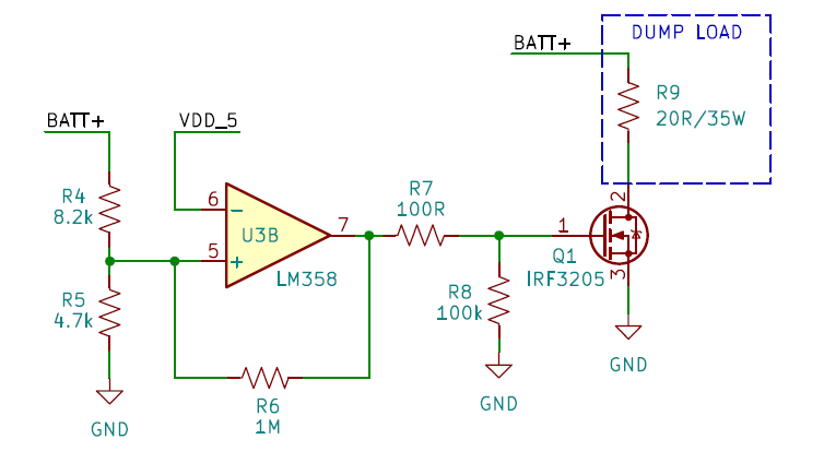
This section uses:
- An LM358 comparator stage
- A battery-voltage divider
- A MOSFET switch
- A 20 Ω / 35 W dump-load resistor
When the battery bus rises above the selected threshold, the comparator turns on the dump-load MOSFET. This connects the resistor across the DC bus and safely dissipates excess regenerated energy as heat.
This protection does not replace the battery as the main energy-storage element, but it provides a safer path for excess energy during regeneration. It also helps protect the MOSFET bridge, capacitors, and battery bus from overvoltage conditions.
The PCB layout was updated to include a large copper area around this resistor and MOSFET section to help with temperature control.
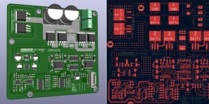
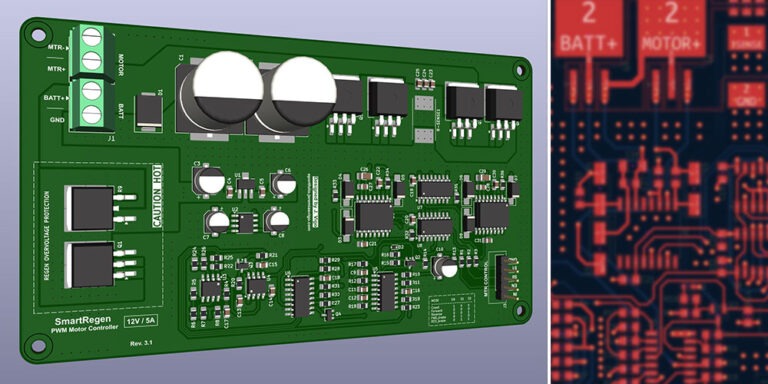
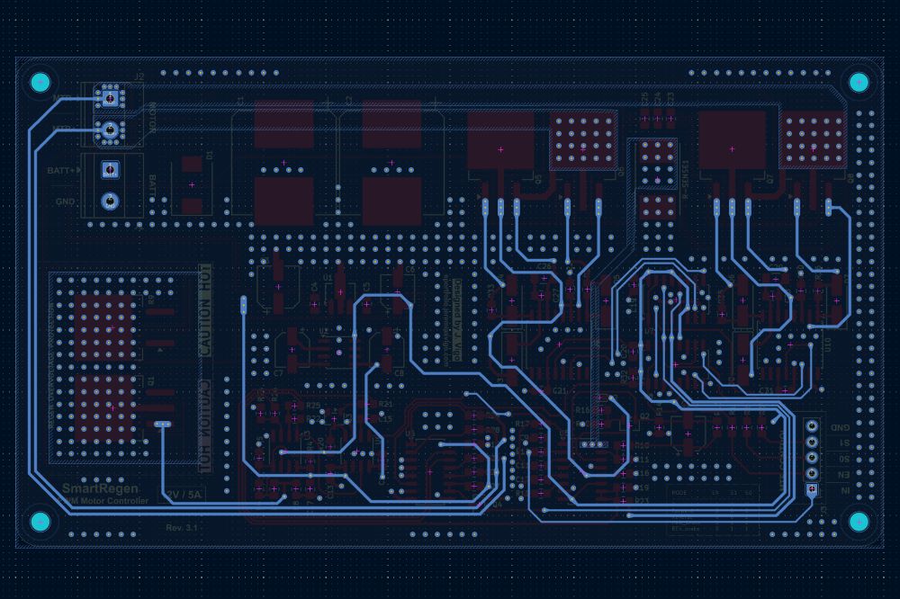
PCB Design
The PCB was designed with power electronics layout considerations in mind. The layout separates the higher-current motor paths from the control circuitry as much as possible. The MOSFETs, gate drivers, current-sense resistor, bulk capacitors, dump-load section, and motor terminals were positioned to keep current paths short and reduce unnecessary loop area.
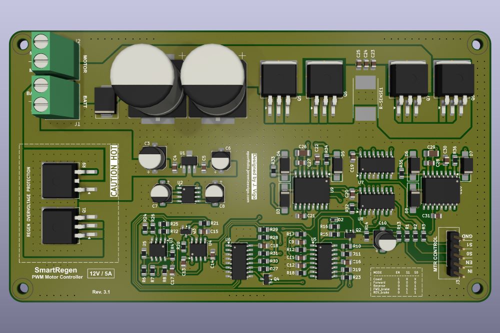
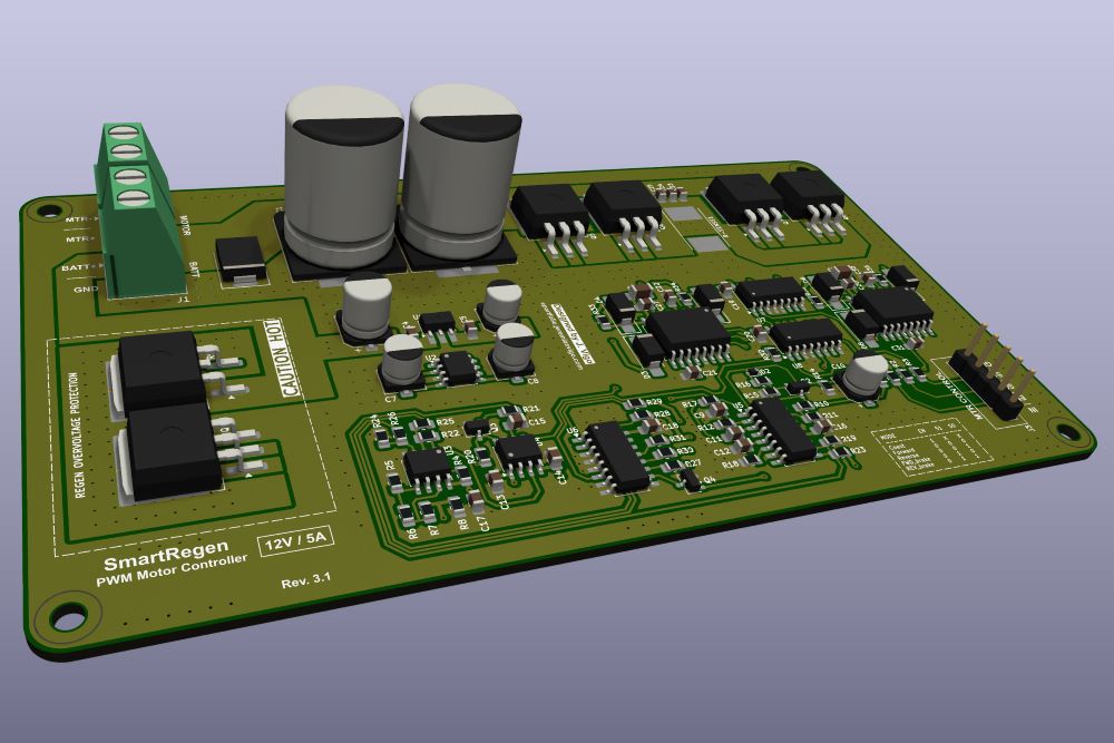
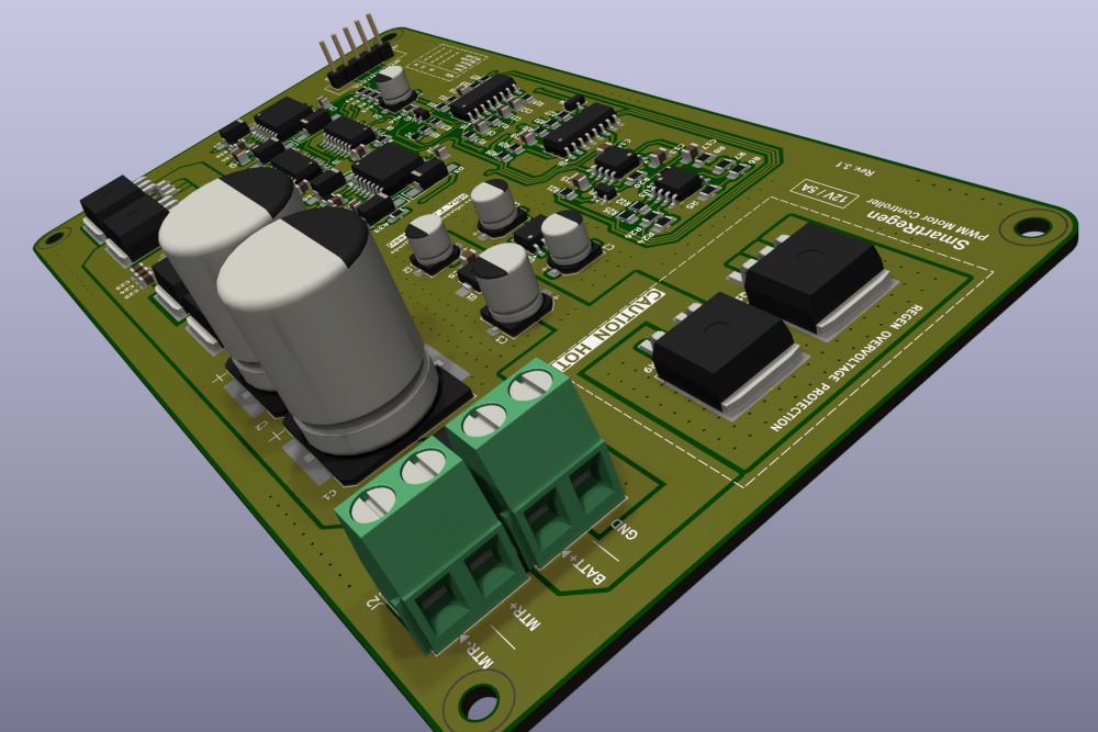
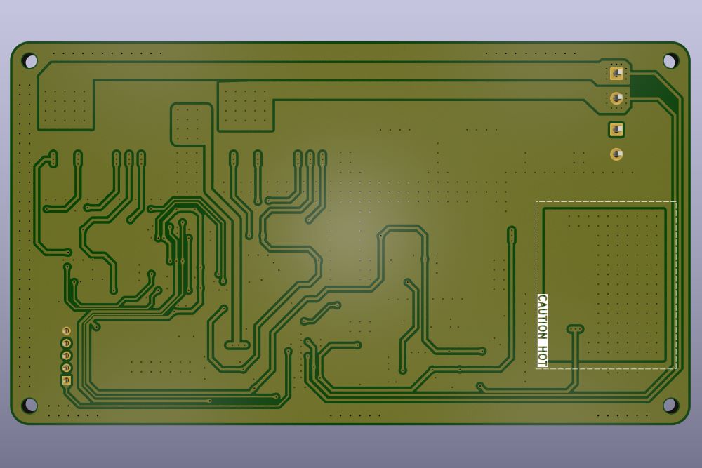
Some of the main layout considerations included:
- Wide copper traces and pours for BATT+, MOTOR+, MOTOR−, and return paths
- Large copper areas near the MOSFETs for heat spreading
- Copper area around the 20 Ω / 35 W dump-load resistor for thermal management
- Local ceramic decoupling near the H-bridge
- Short gate-drive paths between the IR2110S drivers and MOSFET gates
- Current-sense routing kept separate from noisy switching paths
- Clearly labeled connectors for battery, motor, and control inputs
- Silkscreen labels for major functions and operating modes
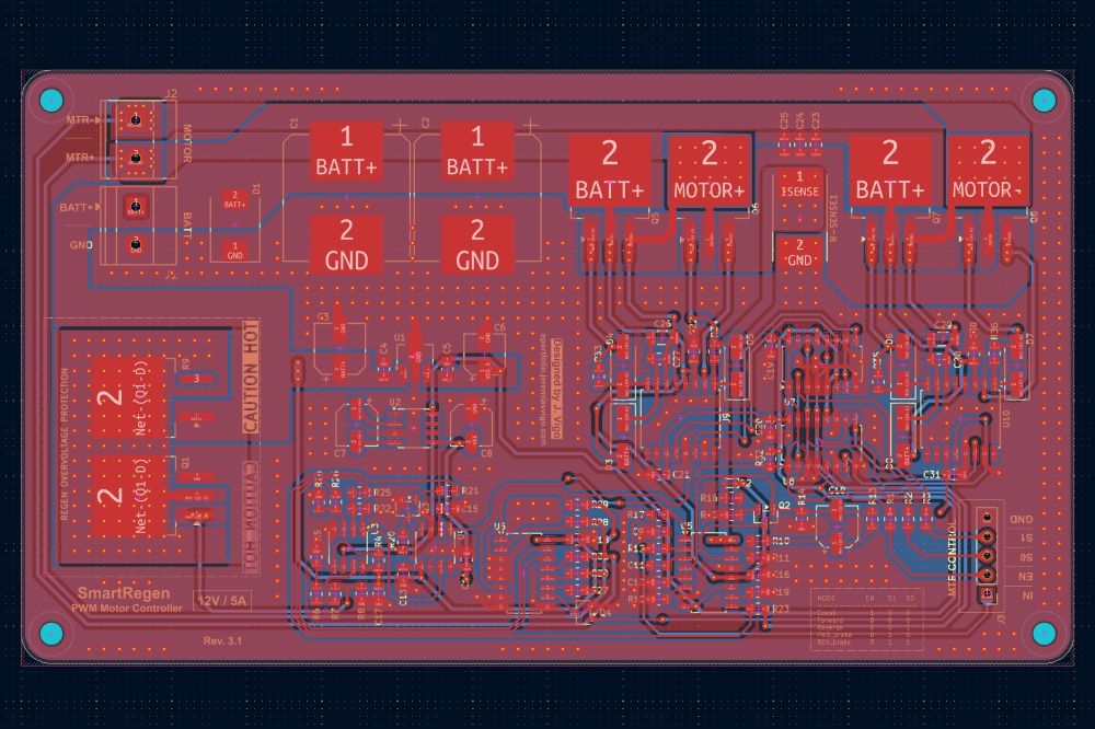
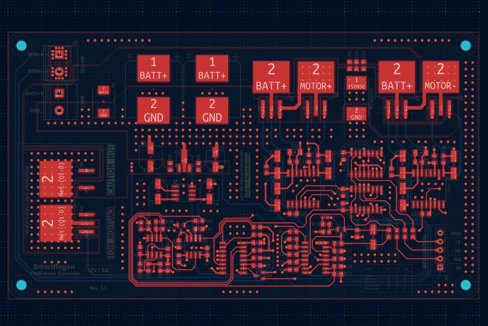
The board also includes silkscreen notes for the key system features:
- PWM Speed Control
- Current Limiting
- Regen Braking
- Bus Overvoltage Protection
What I Learned
This project helped me connect several areas of electrical engineering into one complete design:
- PWM motor control
- Analog feedback control
- Current sensing
- MOSFET gate driving
- H-bridge switching
- Regenerative braking
- Overvoltage protection
- Power-supply decoupling
- PCB layout for power electronics
- Thermal design and copper-area planning
One of the biggest lessons from this design was that a motor driver is not only about building an H-bridge. The feedback polarity, current-sense placement, decoupling, gate-drive routing, thermal paths, and overvoltage behavior all have a major impact on whether the circuit will work reliably with a real motor.
Next Step
The next step is to fabricate the PCB and test the controller with small DC motors before moving toward larger robotics applications. Once the fabricated version arrives, I will update this post with real PCB photos, assembly notes, test results, and any changes needed after hardware validation.
The fabricated PCB photos and testing results will be added as an appendix to this project post.