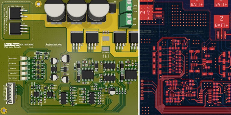
Project Overview
The SmartRegen 10A Motor Controller is a hardware-based PWM DC motor controller designed for bidirectional motor control, current limiting, and regenerative braking. The controller is built around the TL494 PWM controller, discrete logic, MOSFET gate drivers, and a full N-channel MOSFET H-bridge power stage.
The design targets a 12V / 10A operating range, making it suitable for small DC motor applications such as robotics, RC platforms, test benches, educational motor-control systems, and other low-voltage electromechanical projects.
Unlike a microcontroller-based motor driver, this project uses mostly analog and digital hardware to control the motor. The TL494 generates the PWM signal, the SN74153 multiplexers select the correct H-bridge drive signals, the IR2110S gate drivers drive the MOSFETs, and the feedback/protection circuits monitor current, motor voltage, and DC-bus voltage.
The controller supports:
- Forward drive
- Reverse drive
- Coast mode
- Forward regenerative braking
- Reverse regenerative braking
- Current limiting
- DC-bus overvoltage protection
- Manual or external control interface
Main Features
- 12V / 10A target operating range
- TL494-based PWM speed control
- IRF3205 N-channel MOSFET H-bridge
- Dual IR2110S high-side/low-side MOSFET gate drivers
- SN74153 multiplexer-based mode selection
- CD4053 bidirectional feedback switching
- 0.02Ω / 5W current-sense resistor
- 12.8V regenerative overvoltage protection threshold
- 20Ω / 35W braking resistor for dump-load protection
- TVS diode protection across the DC bus
- Three 2200µF bulk capacitors for DC-bus stabilization
- 5V output on the control connector
- Manual control support using switches and potentiometer
- Mode/status indicator LEDs
- Enlarged PCB power traces for high-current paths
Design Goals
The main goal of this project was to design a compact hardware-based DC motor controller capable of driving a 12V motor at up to 10A while also adding protection and regenerative braking features.
The design focuses on several important motor-control requirements:
- PWM speed control
The motor speed is controlled by changing the PWM duty cycle generated by the TL494. - Bidirectional operation
A full H-bridge allows the motor polarity to be reversed for forward and reverse operation. - Current limiting
A low-value shunt resistor measures motor current and feeds the current signal back to the TL494 control loop. - Regenerative braking
The motor can operate as a generator during braking, returning energy back into the DC bus. - Overvoltage protection
A braking resistor circuit activates when the DC bus rises above approximately 12.8V. - Flexible control interface
The control header includes GND, 5V, mode-select inputs, enable input, and speed-control input.
Basic Electrical Ratings
The target operating point for the controller is:
Supply voltage: 12V
Maximum target current: 10A
Maximum electrical input power:
P = V × I
P = 12V × 10A
P = 120W
This 120W value represents the approximate maximum electrical input power available at the 12V / 10A target point. Actual motor output power will be lower because of MOSFET losses, shunt resistor losses, PCB copper losses, switching losses, and motor losses.
Circuit Details
1. DC-Bus and Power Supply
The DC-bus section is the main power input stage of the controller. The battery connects to the board through the BATT+ and BATT− terminals. This supply feeds the H-bridge power stage and also provides input power for the onboard low-voltage regulator.
The DC bus includes a 5KE15CA TVS diode connected across the input. The purpose of this diode is to help clamp voltage spikes caused by motor switching, wiring inductance, and regenerative braking events.
The bus also includes three 2200µF bulk capacitors, giving a total bulk capacitance of:
C_TOTAL = C1 + C2 + C3
C_TOTAL = 2200µF + 2200µF + 2200µF
C_TOTAL = 6600µF
These capacitors provide local energy storage for motor startup, sudden load changes, and PWM switching. They also help reduce voltage dips on the supply rail when the motor current changes quickly.
The low-voltage supply uses an L7805 regulator to generate the 5V logic rail, labeled VDD_5. This 5V rail powers the logic devices and is also available at the control connector for external circuits.
An ICL7660 charge-pump inverter is used to generate the negative rail labeled −VEE. This negative rail is used by the analog feedback circuitry so the system can process bidirectional feedback signals more reliably.
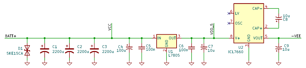
Figure 1. DC-bus input protection, bulk capacitance, 5V regulator, and negative charge-pump supply.
2. TL494 PWM Control Section
The TL494 is the main PWM controller used to generate the motor control signal. The speed command enters the circuit through the CTRL_IN input. This input can be driven by a DC control voltage, a filtered PWM signal, or a manual potentiometer.
The control input represents the target motor speed. The TL494 compares this command signal with the feedback and current-sense signals to adjust the PWM duty cycle.
The circuit includes filtering components at the control input to smooth the command signal before it reaches the TL494. This helps reduce noise and provides a more stable control signal.
The TL494 also receives the ISENSE feedback signal from the shunt resistor. When the motor current increases toward the current-limit point, the TL494 reduces the PWM duty cycle. This protects the MOSFETs, motor, battery, current-sense resistor, and PCB traces.
The TL494 output is routed to the logic selection stage instead of directly driving the MOSFETs. This allows the same PWM source to be applied to different H-bridge inputs depending on the selected operating mode.
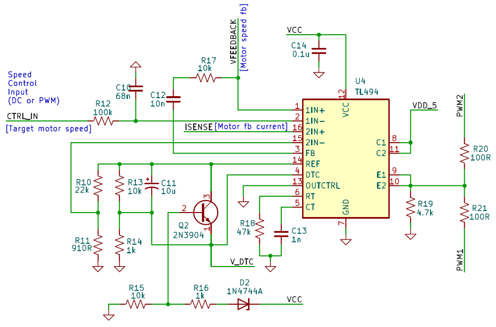
Figure 2. PWM generation, speed command input, feedback input, timing components, and current-limit interface.
3. Current-Sense Resistor and Current Limit
The controller uses a 0.02Ω / 5W shunt resistor in the motor current path. This resistor generates a small voltage proportional to the motor current.
At 10A:
V_SENSE = I × R
V_SENSE = 10A × 0.02Ω
V_SENSE = 0.2V
The power dissipated in the shunt resistor at 10A is:
P = I²R
P = (10A)² × 0.02Ω
P = 2W
A 5W resistor was selected to provide margin above the calculated 2W dissipation. This is important because the shunt resistor can heat up during startup, braking, high-load operation, or motor stall conditions.
The shunt voltage is sent back to the TL494 through the ISENSE signal. When the current increases, the TL494 can reduce PWM duty cycle and limit the motor current.
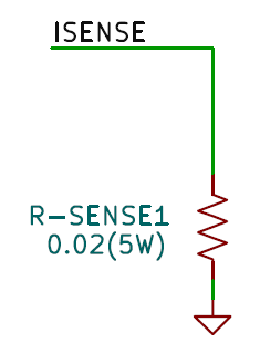
Figure 3. 0.02Ω / 5W shunt resistor used to generate the motor current feedback signal.
4. Mode Selection Logic
The controller uses two SN74153 dual 4-to-1 multiplexers to generate the correct gate-driver input signals for each operating mode.
The mode control inputs are:
- EN
- S1
- S0
The outputs of the mode-selection logic are:
- HL = High-side left
- LL = Low-side left
- HR = High-side right
- LR = Low-side right
These signals are sent to the IR2110S gate drivers, which then drive the MOSFET gates.
The controller supports five operating modes:
| Mode | EN | S1 | S0 | HL | LL | HR | LR |
| Coast | 1 | X | X | 0 | 0 | 0 | 0 |
| Forward | 0 | 0 | 0 | 1 | 0 | 0 | PWM |
| Reverse | 0 | 0 | 1 | 0 | PWM | 1 | 0 |
| FWD_brake | 0 | 1 | 0 | 0 | PWM | 0 | 1 |
| REV_brake | 0 | 1 | 1 | 0 | 1 | 0 | PWM |
In coast mode, all H-bridge drive outputs are off.
In forward mode, one high-side MOSFET and the opposite low-side MOSFET are used to drive the motor in the forward direction.
In reverse mode, the opposite H-bridge diagonal is used to reverse the motor polarity.
In forward regenerative braking and reverse regenerative braking, the switching pattern changes so the motor can slow down while pushing energy back into the DC bus.
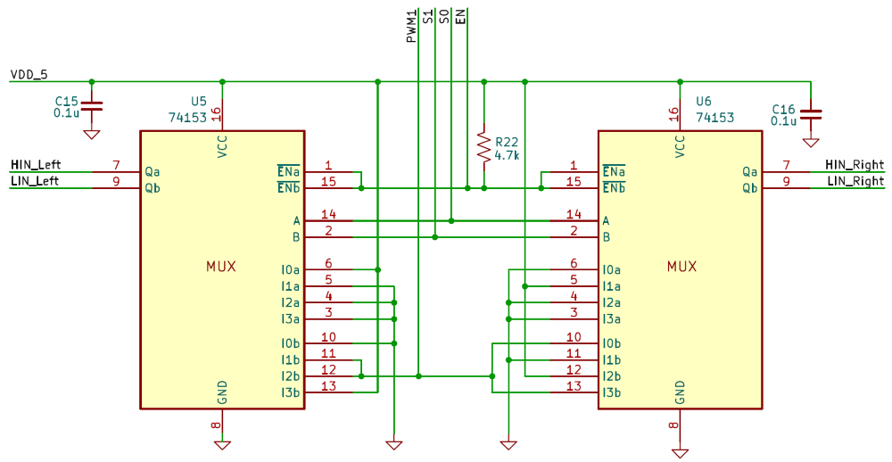
Figure 4. SN74153 multiplexer logic used to route PWM and logic states to the correct H-bridge gate-driver inputs.
5. H-Bridge and Gate-Driver Section
The power stage uses four IRF3205 N-channel MOSFETs arranged as a full H-bridge. This configuration allows the motor terminals to be driven with either polarity, enabling forward and reverse rotation.
Two IR2110S gate drivers are used to drive the MOSFETs. Each IR2110S controls one half-bridge, with one high-side output and one low-side output.
The IR2110S drivers are necessary because the TL494 and logic ICs cannot directly drive the MOSFET gates, especially the high-side MOSFETs. The high-side MOSFET gate must be driven above the motor supply rail to turn on properly. This is handled by the bootstrap network around each IR2110S.
The gate-driver section includes:
- Bootstrap diodes
- Bootstrap capacitors
- Gate resistors
- Gate discharge paths
- Local decoupling capacitors
The gate resistors help limit gate current, reduce ringing, and improve switching stability. The bootstrap capacitors provide the floating supply needed to drive the high-side MOSFETs.
Because the controller is designed for a 10A target current, the H-bridge layout is one of the most important parts of the PCB. The MOSFET current paths must be short, wide, and thermally supported.
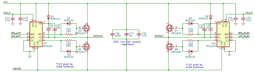
Figure 5. Dual IR2110S gate drivers and IRF3205 MOSFET H-bridge used for bidirectional motor control.
6. Bidirectional Feedback Switching
Because the motor can operate in both directions, the voltage polarity across the motor terminals changes depending on the selected mode. The analog feedback circuit needs a consistent polarity, so the design uses a CD4053 bidirectional analog switch.
The CD4053 selects which motor terminal is routed as the positive feedback input and which terminal is routed as the negative feedback input.
The feedback signals are labeled:
- FB_POS
- FB_NEG
The motor terminals are connected to the CD4053 through 9.1kΩ resistors. These resistors provide input scaling and isolation before the signals enter the analog switch.
A 2N7002 MOSFET is used to condition the control signal for the CD4053. This allows the feedback polarity to follow the selected motor direction.
This section is important because the feedback loop should behave consistently whether the motor is spinning forward or reverse. Without polarity correction, the feedback signal would invert when the motor direction changes.
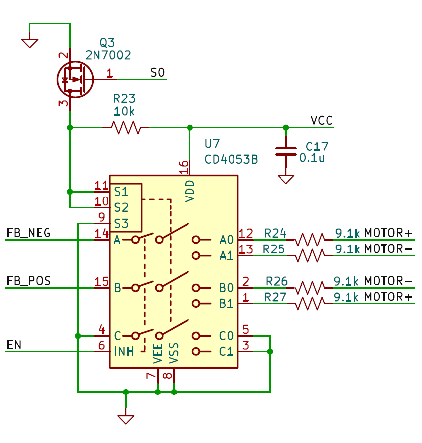
Figure 6. CD4053 analog switch used to select the correct motor-voltage feedback polarity.
7. Voltage Feedback Conditioning
The voltage feedback section processes the motor-voltage feedback before it is sent to the TL494 control loop. This block receives the FB_POS and FB_NEG signals from the bidirectional feedback switch.
An LM358 op-amp stage conditions the differential motor feedback signal. The feedback network scales the motor voltage into a range that can be used safely by the control circuitry.
The design also includes an LF398 sample-and-hold IC. This stage is used to capture and hold the motor feedback signal during the appropriate part of the PWM cycle. This helps produce a more stable feedback signal instead of allowing the feedback loop to react directly to noisy switching waveforms.
The voltage feedback output is labeled VFEEDBACK and is routed back to the TL494 PWM control section.
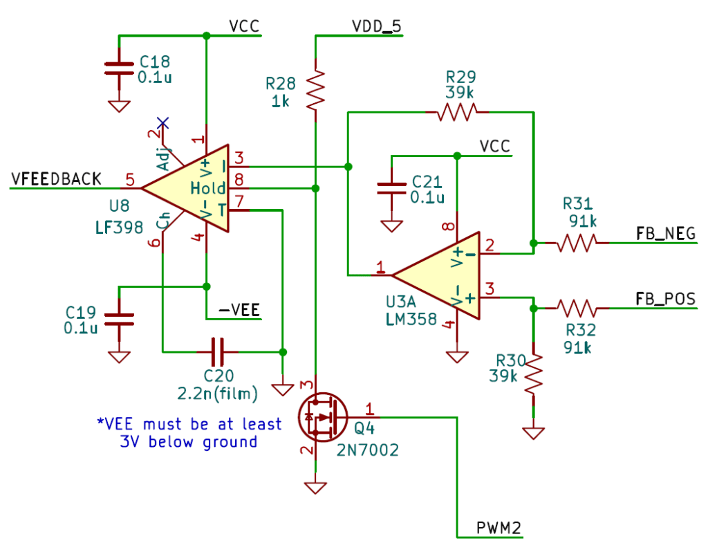
Figure 7. LM358 and LF398 feedback circuit used to condition the motor-voltage feedback signal.
8. Regenerative Overvoltage Protection
During regenerative braking, the motor can behave like a generator. Instead of only consuming energy, it can push energy back into the DC bus. If the battery cannot absorb this energy quickly enough, the bus voltage can rise.
To protect the system, the controller includes a regenerative overvoltage protection circuit.
This section uses an LM358 comparator stage to monitor the battery voltage through a resistor divider. The divider uses:
R_TOP = 28kΩ
R_BOTTOM = 18kΩ
The divided voltage is:
V_DIV = V_BUS × (R_BOTTOM / (R_TOP + R_BOTTOM))
At the 12.8V protection threshold:
V_DIV = 12.8V × (18kΩ / (28kΩ + 18kΩ))
V_DIV = 12.8V × (18kΩ / 46kΩ)
V_DIV ≈ 5.0V
This means the divider produces approximately 5V when the DC bus reaches about 12.8V. The threshold can also be calculated from the 5V reference:
V_BUS_LIMIT = 5V × ((28kΩ + 18kΩ) / 18kΩ)
V_BUS_LIMIT = 5V × (46kΩ / 18kΩ)
V_BUS_LIMIT ≈ 12.8V
When the bus voltage exceeds this threshold, the LM358 output drives the gate of an IRF3205 MOSFET. This MOSFET connects a 20Ω / 35W braking resistor across the DC bus.
The braking resistor dissipates excess regenerated energy as heat. At 12.8V, the approximate braking resistor current is:
I = V / R
I = 12.8V / 20Ω
I = 0.64A
The approximate resistor power at 12.8V is:
P = V² / R
P = (12.8V)² / 20Ω
P ≈ 8.2W
Since the braking resistor is rated for 35W, it provides margin for the expected dump-load dissipation. Thermal performance still depends on airflow, mounting, braking duration, and actual regenerative energy.
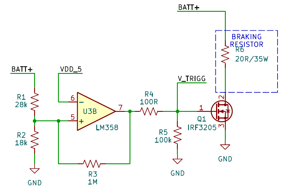
Figure 8. LM358 comparator, IRF3205 MOSFET, and 20Ω / 35W braking resistor used for DC-bus overvoltage protection.
9. Mode and Status Indicator LEDs
The controller includes display LEDs to show important operating states. These LEDs make testing and troubleshooting easier because the user can quickly see which control state is active.
The indicator LEDs include:
- OVP ACTIVE
- PWM CUTOFF
- FORWARD MODE
- REVERSE MODE
- REGEN MODE
These indicators are useful during bench testing because they help confirm that the mode-selection logic, protection circuit, and PWM cutoff behavior are working as expected.
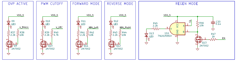
Figure 9. Indicator LEDs for OVP active, PWM cutoff, forward mode, reverse mode, and regenerative braking mode.
10. Manual Control Setup
The control connector provides a simple interface for external control. It includes:
- GND
- 5V output
- S1
- S0
- EN
- CTRL
For manual testing, the mode pins can be connected to switches with pull-down resistors. The CTRL input can be connected to a potentiometer to adjust the PWM speed command.
The added 5V output allows the control connector to power simple external circuits, pull-ups, or a small MCU interface, as long as the current drawn from the onboard 5V regulator stays within a safe range.
This setup makes it possible to test the board without needing a microcontroller. The user can manually select coast, forward, reverse, forward braking, and reverse braking modes.
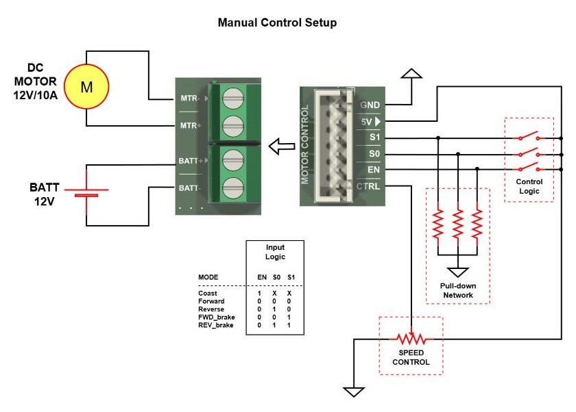
Figure 10. External switch and potentiometer wiring for manual control of motor direction, braking mode, enable, and speed command.
PCB Design
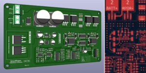
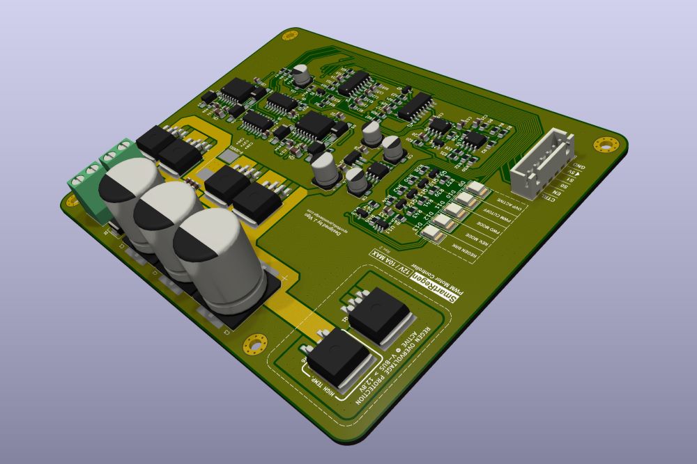
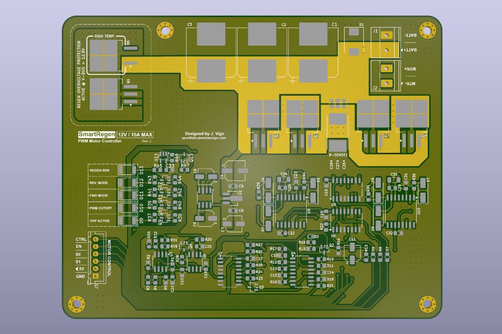
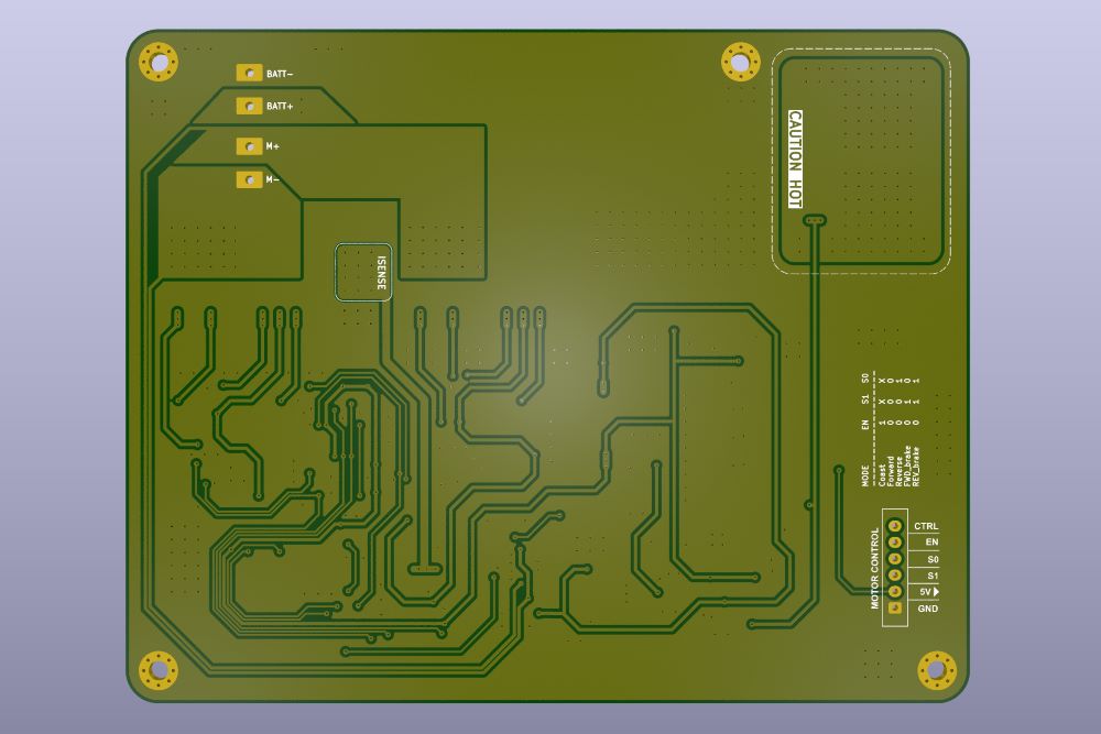
The PCB layout was designed around the high-current motor path first. Since the controller targets 10A operation, the BATT+, BATT−, MOTOR+, MOTOR−, MOSFET bridge, current-sense resistor, and braking resistor paths were given priority in the layout.
The power traces were made significantly wider to reduce voltage drop, resistive heating, and current crowding. Sensitive analog and feedback traces were routed separately from the noisy switching paths to reduce unwanted coupling into the TL494 feedback loop.
The layout also includes mounting holes, labeled connectors, a separated braking resistor area, bulk capacitors near the DC bus, and clearly marked control/status sections.
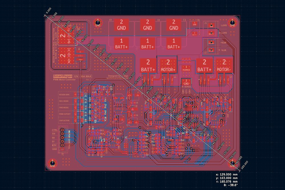
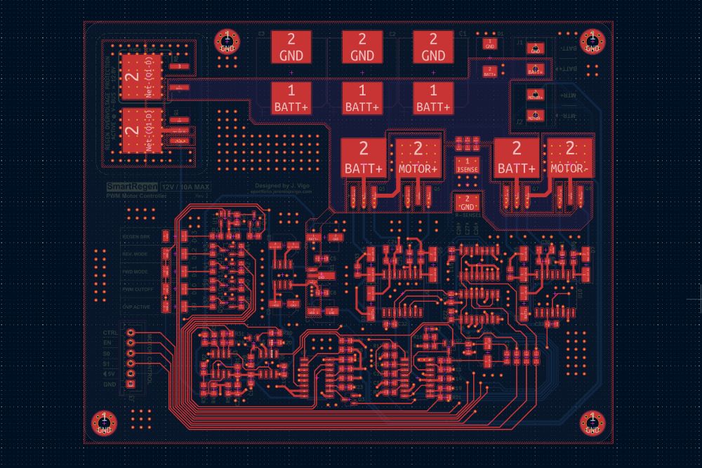
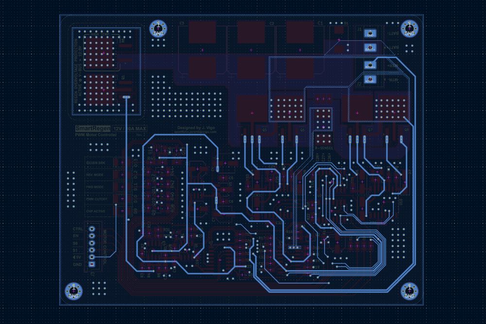
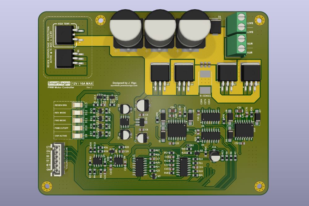
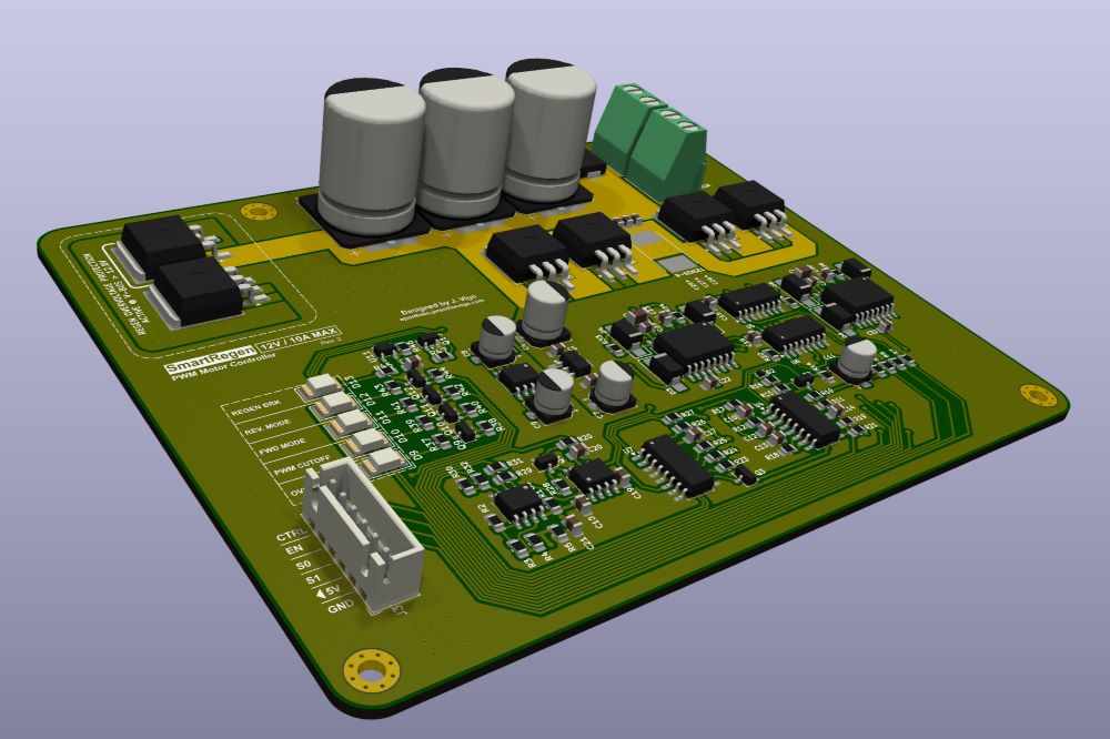
The 3D PCB simulations were used to verify the physical arrangement of the board before fabrication. These views help check component spacing, connector placement, capacitor clearance, MOSFET positioning, braking resistor placement, and overall board readability.
The 3D views are especially useful for confirming that the high-current power section, control section, and protection section are physically organized in a practical way.
Next Steps
The next step is to fabricate and assemble the PCB for hardware testing.
Initial testing will be done with a current-limited bench supply before connecting a larger motor load. The first tests will focus on verifying the power rails, TL494 oscillator, PWM output, control inputs, mode-selection logic, gate-driver outputs, and indicator LEDs.
After the basic control signals are verified, the H-bridge will be tested with a small DC motor at low current. Higher-current testing will be performed gradually while monitoring MOSFET temperature, shunt resistor temperature, braking resistor temperature, DC-bus voltage, and PWM behavior.
Planned validation tests include:
- 5V regulator output verification
- −VEE charge-pump output verification
- TL494 PWM frequency and duty-cycle range
- Forward and reverse drive modes
- Coast mode
- Forward regenerative braking
- Reverse regenerative braking
- 10A current-limit behavior
- 12.8V overvoltage protection activation
- Braking resistor activation
- Mode/status LED operation
- Thermal behavior of MOSFETs, shunt resistor, and braking resistor
- Voltage drop across high-current PCB paths
Once the board is assembled and tested, the project can be updated with real PCB photos, oscilloscope captures, motor test results, thermal measurements, and any design improvements discovered during hardware validation.